1. Background
1.1. Differential and common-mode
Differential signaling using a pair of wires is highly useful for sending signals between circuits. It makes it possible to remove several types of noise and interference added to the signal along its path from transmitter to receiver. USB and wired Ethernet connections are common examples of differential signaling in practice.
The desired signal is applied as the difference between the two wires and, ideally, the noise voltages/currents are added equally and in-phase to each conductor of the pair. The receiver simply takes the difference of the pair as the signal quantity, therefore removing all of the noise.
There are 3 nodes that participate in a differential pair of signals: a common reference defined at the receiver’s end of the circuit, and the two signal nodes A and B (or [+in and -in], or [inp and inm]) The node voltages Va and Vb (measured with respect to the circuit’s reference node) completely describe the values.
However, it is much more useful to define another set of quantities:
Given the set of differential and common-mode voltages for a pair of nodes, it is a small matter of algebra to know the individual node voltages:
See Figure 1, “Two ways of specifying the voltage at a pair of nodes.” for a graphical version of these conversion equations.

- Some additional points to remember
-
-
In either system, two terms are required to completely specify the potentials at the two nodes.
-
The equations use terms in lowerUPPER notation, the total or physical quantity, to emphasize that these two systems are always valid.
-
… meaning they are also valid for DC quanitities (UPPERUPPER notation) and for small-signal quantities (lowerlower notation).
-
2. Lab goals
In this lab you will construct a simple 3-stage operational amplifier from discrete components and begin measuring the DC and low-frequency performance of your unit. It will provide a real-world example for our study of the major opamp specifications which are useful in selecting an appropriate part during the design process.
Reminder: we are using the AD2 specifically because they are able to output two phase-locked waveforms and the input channels are differential. There is no need to use "Math" to subtract channel 2 from channel 1 → just directly attach the two wires of each channel to the two nodes that are to be subtracted.
3. Procedure
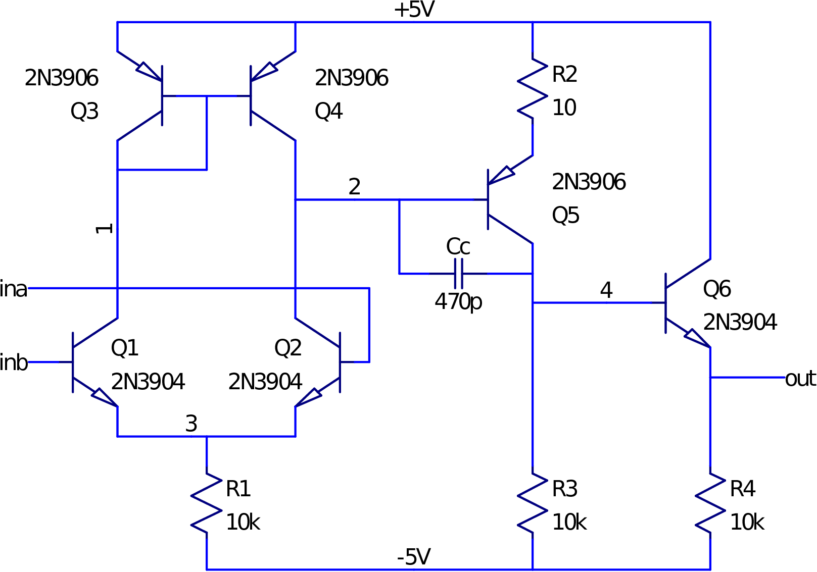
Construct the opamp of Figure 2, “Discrete opamp schematic” on a small section of breadboard.
The capacitor Cc helps to stabilize this amplifier, but you can greatly help the situation by minimizing the length of jumper wires used in the construction.
-
Be sure to allow yourself easy access for replacing capacitor
Ccand for attaching meters to nodesina,inb, andout. -
Use the physically small ceramic capacitor types for
Cc. -
Add a large capacitor (1 to 10 μF) between the
VccandVeenodes to help reduce the effect of the long wires connecting to the power supply. -
For each of the 3 npn transistors: use the “diode check” mode on the multimeters to measure VBE. Select the transistors with the closest values as
Q1andQ2. Since VBE is sensitive to temperature changes, it is best to minimize touching the transistors until you’ve measured them (use pliers). -
Do a similar procedure to select your
Q3andQ4pair.
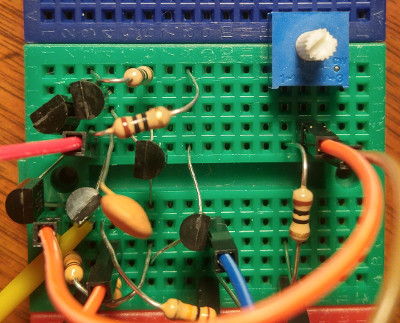
See Figure 3, “Compact construction example” for an example of pre-bending transistor leads and building the circuit in the same general arrangement as the schematic. This makes troubleshooting easier since the geometry is similar and reduces the parasitic inductances and the electric and magnetic coupling between nodes and loops.
Several of the resistors are bent to be in a vertical position.
Bend and trim your resistor leads as shown in Figure 4, “Vertical
resistor”.
The right lead in the figure makes for a convenient loop for attaching probes.
resistor
-
Attach the +5V and -5V power supply connections to your amplifier.
-
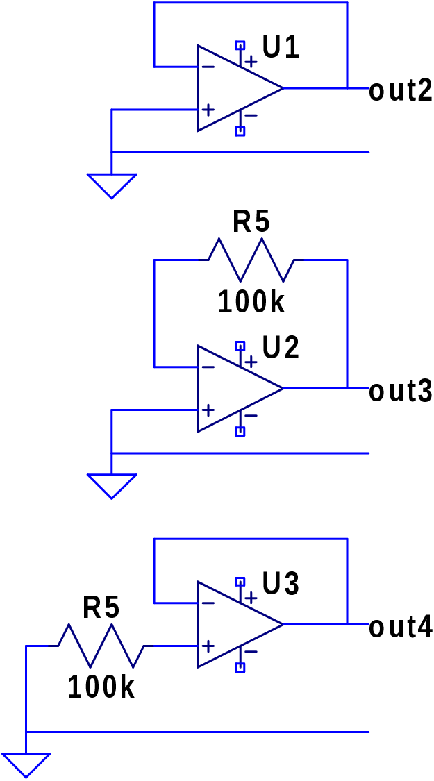
Add external wires to connect your opamp as show in the first circuit of Figure 5, “Amplifier connections” — an amplifier with voltage gain of 1 with a 0 V input. These wires are OK to be long.
-
Measure the internal node voltages of your amplifier (nodes
1,2,3,4, and alsoout2) with respect to GND. Display the output node on an oscilloscope to verify that the amplfier is not oscillating then use the benchtop multimeters for the DC measurements. -
Compare these voltages to your predicted values from the circuit analysis done for
hw10. Also estimate the transistor collector currents. (the analysis conditions were: Vina = Vinb = Vout = 0 V)
Name |
Value |
Vout |
|
V1 |
|
V2 |
|
V3 |
|
V4 |
|
IR1 |
|
IR3 |
|
IR4 |
Then, as a next step, use an AD2 input channel or the nice DMMs in the lab. First, connect your probes to the same node in your circuit (such as out2), change the vertical scale to show the resulting, should-be-zero-but-isn’t, noisy signal, and measure its DC value (average not DC RMS) in Waveforms. This offset value is effectively added to every measurement you make when using this same vertical scale and offset settings. This number must then be subtracted from your other measurements to get the true node voltage. For example: The short-circuit value measured to be +2.8 mV. Using the same channel and scale settings, your meter (or Waveforms) says node out2 is -5.3 mV. The true node voltage is (-5.3 mV - 2.8 mV) = -8.1 mV. Not compensating for the measurement instrument’s offset would give you a 35% error! (-8.1 - (-5.3))/-8.1 * 100 = 35. |
3.1. Construct all circuits of Figure 5, “Amplifier connections”
Measure the value of your 100 kΩ resistor to 3 digits using the multimeter. Use this same unit for all parts of Figure 5, “Amplifier connections”
-
For each of the configurations, use the benchtop multimeter to measure the following DC voltages:
-
VoutX
-
Vina (+ input)
-
Vinb (- input)
-
VR5, the voltage across resistor
R5
-
4. Make an opamp-based amplifier!
4.1. Non-inverting
Can you make an opamp-based amplfier with a voltage gain of +10 V/V? Use your opamp instead of a chip!
The feedback network’s resistance as seen by the opamp’s output should be greater than 5× 10 kΩ since the current sinking performance is limited by the internal 10 kΩ R4.
Demonstrate this by amplifying a 1 kHz input signal which is centered around 0 V.
-
What is the maximum signal input amplitude?
-
What is the maximum input signal amplitude when configured for a +1 V/V gain?
References
-
[[[341-notes]]] D. White, ECE 341 Class notes 2019 folder, https://drive.google.com/drive/folders/1vzdLxzTUAC6xXF6YjVcDRuy_BKR7gzDz?usp=sharing
-
[[[341-docs]]] D. White, ECE 341 reference documents folder, https://drive.google.com/folderview?id=0B5O5cSaA0tEQYVpaSnJxMGFrdHM
-
[AoE] P. Horowitz and W. Hill, The Art of Electronics 3rd ed. (affiliate link), Cambridge University Press, 2015. https://artofelectronics.net
-
[L-AoE] T. Hayes, Learning the Art of Electronics: A Hands-On Lab Course (affiliate link), Cambridge University Press, 2016. https://learningtheartofelectronics.com
-
[LEC] Tony R. Kuphaldt, Lessons in Electric Circuits, Source version: https://www.ibiblio.org/kuphaldt/electricCircuits/, All About Circuits version: https://www.allaboutcircuits.com/textbook/
-
[CL-book] Michael F. Robbins, CircuitLab, Ultimate Electronics: Practical Circuit Design and Analysis, https://www.circuitlab.com/textbook/
-
[TCA] Alfred D. Gronner, Transistor Circuit Analysis, Simon & Schuster, 1970, https://archive.org/details/TransistorCircuitAnalysis
-
[CMOS VLSI] Neil Weste and David Harris, CMOS VLSI Design - A Circuit and Systems Perspective, 4th edition. Addison-Wesley, 2011. http://pages.hmc.edu/harris/cmosvlsi/4e/index.html
-
[Guidebook] D. White, Guidebook for Electronics II. https://agnd.net/valpo/341/guidebook
-
[Gummel-Poon] H.K. Gummel, H.C. Poon, An Integral Charge Control Model of Bipolar Transistors. Bell System Technical Journal, 49: 5. May-June 1970 pp 827-852. https://archive.org/details/bstj49-5-827
-
[ROHM] ROHM Semiconductor, Electronics Basics, http://www.rohm.com/web/global/en_index
-
[vishay-e-series] Vishay, Standard Series Values in a Decade for Resistances and Capacitances, https://www.vishay.com/docs/28372/e-series.pdf