1. Review
- Equilibrium
-
-
Open circuit
-
Depletion region forms with separated and fixed-in-place charges, setting up an internal E-field.
-
Built-in potential \(V_0\).
-
- Reverse bias
-
-
Same direction as the built-in field and \(V_0\).
-
No real change in current (≈0).
-
Depletion width increases with more reverse bias.
-
Effect is a voltage-variable capacitance.
-
2. Forward bias
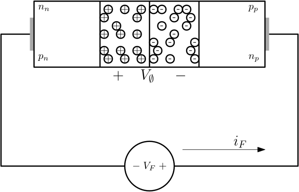
Revisit the built-in potential:
Solve for the minority carrier concentrations in equilibrium:
-
\(p_n (\text{equ}) = \)
-
\(n_p (\text{equ}) = \)
| The barrier (\(V_0\)) is reduced by the external applied voltage VF since they are in opposite directions. |
We can compute the new minority carrier concentration by replacing \(V_0 \Rightarrow V_0 - V_F\).
-
\(p_n (\text{fwd}) = \)
-
\(n_p (\text{fwd}) = \)
Details
\(p_n (\text{fwd}) = \dfrac{p_p}{\exp\left(\dfrac{V_0 - V_F}{V_T}\right)}\)
2.1. Towards current flow
|
ONLY the minority carriers are affected. → the pn junction is a minority carrier device. |
The change in hole concentration is:
Collect the terms with V0
Details
What we know:
-
np and pn increase exponentially lots,
-
diffusion currents therefore also increase lots.
{ … insert another day or so of semiconductor physics … }
We also know that:
-
Total current is proportional to this change in minority carrier concentration,
-
\(I_\text{total} \propto \left(\Delta p_n + \Delta n_p\right)\)
So:
Circle all of the parts where temperature is buried.
2.2. Shockley diode equation
The −1 makes things difficult, can it be dropped? Continue here.