$\huge \texttt{FOLLOW THE CHANNEL}$
Structure and notation
The gate is the main terminal in the operation of a MOSFET, therefore there are three voltages to keep track of:
$\hspace{1em}$ $v_{GS}$ $\hspace{1em}$ $v_{GD}$ $\hspace{1em}$ $v_{GB}$
Also, don't forget about the two pn junctions in the structure. It is usually bad to forward-bias those junctions.
$\hspace{1em}$ $v_{SB}$ $\hspace{1em}$ $v_{DB}$
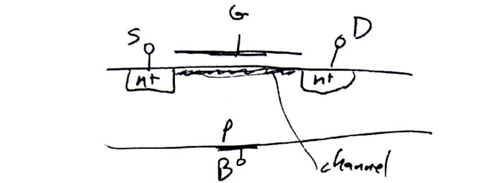
The potential $v_{GB}$ is only useful in accumulation and depletion modes and not useful (for this first pass) when the region under the gate terminal (the channel) is inverted, or has an induced layer of free charge carriers. In inversion, the conductive layer of charge acts as an electrostatic shield, preventing the gate's potential to affect the E-field between the channel and the body terminal.
For the time being, only consider the two voltages $v_{GS}$ and $v_{GD}$.
From the side view of this setup, make a new voltage $v_{ox}(x)$, the (vertical) potential between the gate and the channel along the path from source to drain terminals. The end points of this function are $v_{ox}(0) = v_{GS}$ and $v_{ox}(L) = v_{GD}$.


In Art of Electronics, page 136, footnote 10: Pay attention to the subtle difference between definitions of threshold voltage for a MOSFET.
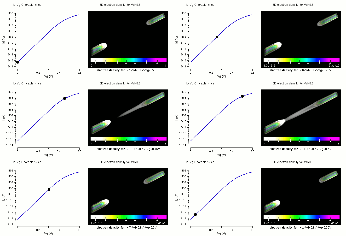
The animation here is a nice illustration of charge in a MOSFET channel: (clickable link!) Wikipedia: Threshold Voltage
The figures in A review of recent MOSFET threshold voltage extraction methods do a good job of showing how to find $V_{TN}$. Pay attention to the asymtote lines in Fig. 3, 4, and 6.

Horizontal current flow $(i_D)$
Begin by calculating the charge contained in the inversion layer (channel) as a function of position:
\begin{equation} \underbrace{Q(x)}_{\mathrm{C\cdot cm}} = -1 \cdot W \cdot C_{ox} \cdot \underbrace{\left(v_{ox}(x) - V_{TN} \right)}_{v_{OV}} \end{equation}
- For an n-channel MOSFET, the channel charge is electrons.
- $C_{ox} = \dfrac{\epsilon_{ox}}{t_{ox}}$. Remember $\epsilon_{ox} = \epsilon_{r,\,SiO_2} \epsilon_0$ with $\epsilon_{r,\,SiO_2} = 3.9$
- $v_{OV}$ is the "overdrive" voltage, the excess potential over that required to create a channel ($V_{TN}$).
- Since the gate is a conductor, its charge (positive, attracting the channel charge) is evenly distributed.
Also, a substitution which will be used shortly:
\begin{equation} v_{ox}(x) = v_{GS} - v_c(x) \end{equation}
where $v_c(x)$ is the potential at position $x$ along the channel with respect to the S terminal. Therefore $v_c(0) = 0$ and $v_c(L) = v_{DS}$.
Current is moving charge
\begin{align} i(x) &= Q(x) \cdot \vec{v}_x(x) \\ &= \left[-W C_{ox} \left(v_{ox}(x) - V_{TN} \right)\right] \left[-\mu_n \vec{E}_x(x) \right] \end{align}
Remember that the E-field is $\vec{E}_x(x) = - \dfrac{\mathrm{d}\, v_c(x)}{\mathrm{d}\, x}$.
So many minus signs... Integrate both sides like:
\begin{equation} \int\limits_0^L i(x)\, dx = \int\limits_0^{v_{DS}} -\mu_n C_{ox} W \left(v_{GS} - v_c(x) - V_{TN} \right) \, d v_c(x) \end{equation}
We are assuming that all current is flowing horizontally and not leaving the channel. Therefore $i(x)$ must be constant.
\begin{align} L \cdot i_D &= \cdots \\ i_D &= \mu_n C_{ox} \dfrac{W}{L} \left(v_{GS} - V_{TN} - \dfrac{v_{DS}}{2}\right) v_{DS} \\ \longrightarrow \; i_D (\text{triode}) &= \mu_n C_{ox} \dfrac{W}{L} \left[ \left(v_{GS} - V_{TN}\right) v_{DS} - \dfrac{v_{DS}^2}{2} \right] \end{align}
Some observations and comments about this equation:
It is valid only if there is a channel present all the way across the length.
- There is a channel if $v_{ox}(x) > V_{TN}$.
- Another way: $(v_{GS} - v_c(x)) > V_{TN}$ for $0 \le x \le L$
- remember $v_c(L) = v_{DS}$
- Combining, we get three equivalent conditions:
- $(v_{GS} - v_{DS}) \ge V_{TN}$
- $(v_{GS} - V_{TN}) \ge v_{DS}$
- $v_{DS} \le v_{OV}$. Remember $v_{ov} = (v_{GS} - V_{TN})$
$\frac{W}{L}$ is the aspect ratio of the transistor
- and is under control of the designer
$\mu_n C_{ox} = k'_n$ - process trans-conductance parameter
$k_n = k'_n \frac{W}{L}$
FOLLOW THE CHANNEL is the best advice for understanding FETs. Always be clear about if, when, and where there is a channel in the device.
Channel pinch off
As $v_{DS}$ is increased (for a constant $v_{GS}$), the channel thickness decreases at the drain side. The channel is now wedge shaped.
When the voltage between the gate and drain $v_{GD}$ decreases low enough to equal $V_{TN}$, the channel depth drops to zero. This condition forms the boundary ("locus" in the slide) between triode mode and saturation mode.
Operation modes
$\huge \texttt{FOLLOW THE CHANNEL}$
Decoder table: "Is there a channel on the {S, D} side?"
| $v_{GS} \downarrow$ $v_{GD} \rightarrow$ | $\ge V_{TN}$ | $\le V_{TN}$ |
|---|---|---|
| $\ge V_{TN}$ | triode | saturation |
| $\le V_{TN}$ | saturation | cutoff |
| BJT | MOSFET | typical use |
|---|---|---|
| cutoff | (cut)off | OFF switch |
| forward active | saturation | amplifier |
| saturation | triode | ON switch |
| reverse active | saturation | FETs can be symmetric |
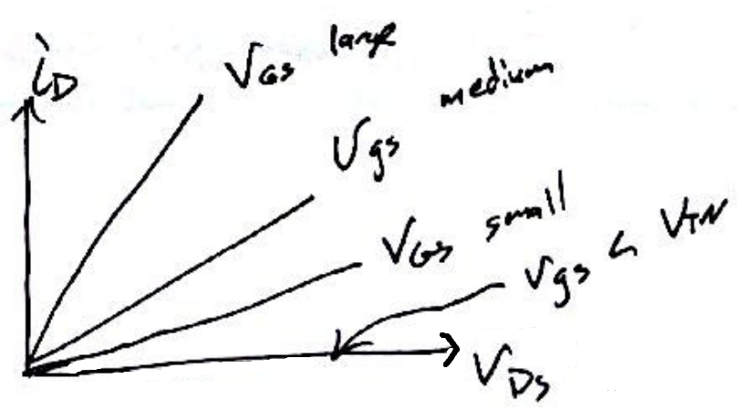
Voltage-controlled resistance
Remember how you could view a pn junction diode as a current-controlled resistance (Lab 4)?
\begin{equation} \underbrace{\dfrac{\mathrm{d}\, i_D}{\mathrm{d}\, v_{DS}}}_{\text{conductance}} = \mu_n C_{ox} \dfrac{W}{L} v_{OV} - v_{DS} \end{equation}
Around $v_{DS} = 0$, we can drop the last term and end up with a conductance:
\begin{equation} g_{DS} = \mu_n C_{ox} \dfrac{W}{L} v_{OV} \end{equation}
or an incremental resistance:
\begin{equation} r_{DS} = \dfrac{1}{g_{DS}} = \dfrac{1}{\mu_n C_{ox} \frac{W}{L} v_{OV}} = \dfrac{1}{\mu_n C_{ox} \frac{W}{L} \left(v_{GS} - V_{TN}\right)} \end{equation}
This is a voltage-controlled resistance!
When using a MOSFET as a switch, $v_{GS}$ is merely made large, along with the ratio $W/L$, to minimize the ON-state resistance. Electrically controlled resistances find use in linear circuits such as variable attenuators and tunable filters.

