Name:
Honor Code:
Instructions
These pages should contain your final solution (setup, reasonable amount of intermediate work, and clearly-indicated answer) and be void of cross-outs, partial pencil erasures, and other clutter.
Print replacement pages and re-assemble if necessary. It is recommended to do your initial solution on engineering paper and transfer the final version here.
-
You may use your book or other reference and computational resources as you see fit.
-
Help from other humans besides the instructor is forbidden.
-
If you use AI-related resources, say so clearly and describe what and how you used those tools to assist your work.
1. BJT transistor circuit
Assume \(V_{BE}=0.6\,\mathrm{V}\) for each transistor in the circuit.

-
i_9=
-
\(i_{\text{Emitter 1}}\) =
-
\(V_{XZ}\) =
2. Pulse generator

-
For \(t<0\), V1 = 0 V.
-
At \(t=0\), V1 0→5 V rising edge.
-
For \(t>0\), V1 = 5 V.
Using graph paper or similar, draw the voltage waveforms at all nodes for time from just before t=0 until the end of the pulse at node out.
-
in -
base of
Q1(label itb1if you wish) -
c1,b2,out
Label all vertical and horizontal axes with appropriate units and to scale. Show the equations that govern the shapes of each portion of the waveforms.
3. MOSFET operating conditions
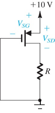
-
\(k_p = \mu_p C_{ox} \dfrac{W}{L} = 200 \,\dfrac{\mu A}{V^2}\)
-
\(V_{\mathrm{TP}} = 1.8\,\mathrm{V}\) (i.e. VSG at the threshold)
What value of R causes this transistor to operate at the boundary between triode and saturation modes?
4. CMOS inverter
Use the given CMOS inverter schematic and the simulation results on the last page for the following questions

4.1. Load capacitance
Estimate the value of capacitor C1 using the simulation waveforms.
Show that both the output falling edge and output rising edge yield values within 20% of each other.
4.2. Input 0
-
Assume enhancement type transistors with threshold voltages \(0 < V_{TN, GS} < 1.2\) and \(0 < V_{TP, SG} < 1.2\).
Find the transistor voltages at t=0:
-
\(V_{GS\,1}\) =
-
\(V_{DS\,1}\) =
-
\(V_{GD\,1}\) =
-
Is there a channel on the source side of
M1? because -
Is there a channel on the drain side of
M1? because
-
\(V_{GS\,2}\) =
-
\(V_{DS\,2}\) =
-
\(V_{GD\,2}\) =
-
Is there a channel on the source side of
M2? because -
Is there a channel on the drain side of
M2? because
4.3. Input 1
-
Assume enhancement type transistors with threshold voltages \(0 < V_{TN, GS} < 1.2\) and \(0 < V_{TP, SG} < 1.2\).
Find the transistor voltages at t=180 ps:
-
\(V_{GS\,1}\) =
-
\(V_{DS\,1}\) =
-
\(V_{GD\,1}\) =
-
Is there a channel on the source side of
M1? because -
Is there a channel on the drain side of
M1? because
-
\(V_{GS\,2}\) =
-
\(V_{DS\,2}\) =
-
\(V_{GD\,2}\) =
-
Is there a channel on the source side of
M2? because -
Is there a channel on the drain side of
M2? because
4.4. Threshold voltages
Use the simulation’s waveforms to estimate the threshold voltage of each transistor. \(V_{TP,\,SG}\) and \(V_{TN,\,GS}\)
Describe your reasoning, labeling points on the waveforms (specific time, voltage, current values) to support your determination.
4.5. Performance coefficients
Estimate each transistor’s performance parameter \(k_{n,p} \left(= \mu_{n,p} C_{ox} \frac{W}{L} \right)\). Report the values in units of \(\dfrac{\mu A}{V^2}\). Describe your process, reasoning, and steps to arrive at these numbers including marking points on the simulation waveforms.
5. MOSFET pins
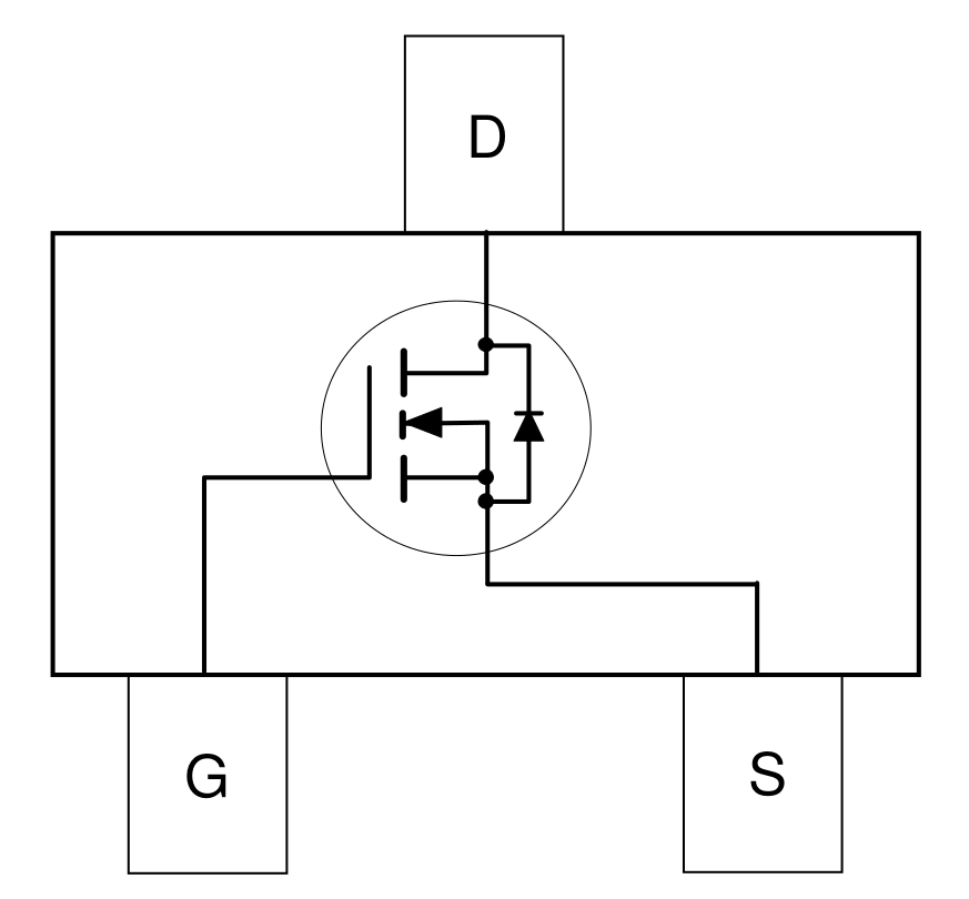
The figure shown is from the datasheet for the BSS138 N-channel MOSFET. Notice that the diode is drawn inside the transistor symbol.
-
Explain why this diode is already and always present in the MOSFET’s structure — it is not an added part between the D and S terminals.
-
There are actually two pn junctions in a MOSFET. Explain why this figure only draws one. Describe which pn junction diode symbol represents and which junction is not shown in the figure.
6. I2C level converter

This is a common method of level-shifting an I2C bus connection between devices using different power supply voltages.
-
Why does the circuit no longer work properly if the two power supply connections +3.3 V and +5 V are swapped? (equivalently: if the transistor is put in "backwards" by swapping the drain and source connections)
