In this lab, we will measure the current-voltage characteristics of pn junction diodes, learn about preferred numbers, and send signals through several diode circuit configurations.
1. Hardware
-
Analog Discovery 2 with Waveforms (tested with
v3.16.3) -
Adjustable power supply, 0—20 V [1]
-
1N4148or1N914Asilicon pn junction diode "small signal switching" -
1N4004silicon pn junction diode "standard rectifier" -
1N34Aor1N270germanium pn junction diode (these are not common or cheap, please return when done) -
BZX79C3V6silicon pn junction 3.6 V zener diode -
various resistors
2. Task 0: See the answer first
| Est. time |
15 min |
Connect your AD2 to your computer and start the WaveForms software.
From the Welcome tab, select the Tracer tool.
Notice the small schematic in the upper-right side of the window? This is the schematic that WaveForms is assuming that you have hooked up to the AD2’s pins. Go ahead and make it so.[2] Your lab partner’s duty is to actually verify, with their own eyes, that you have wired this correctly.
Change the settings to match the figure below, specifically:
-
No Adapter
-
Diode
-
Set R to the value of resistor you are currently using (start with 1 kΩ)
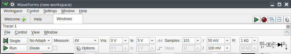
Click the Run button to start sending and receiving data. If you have your diode in the correct way (the package stripe usually matches the symbol bar) your display will look like:
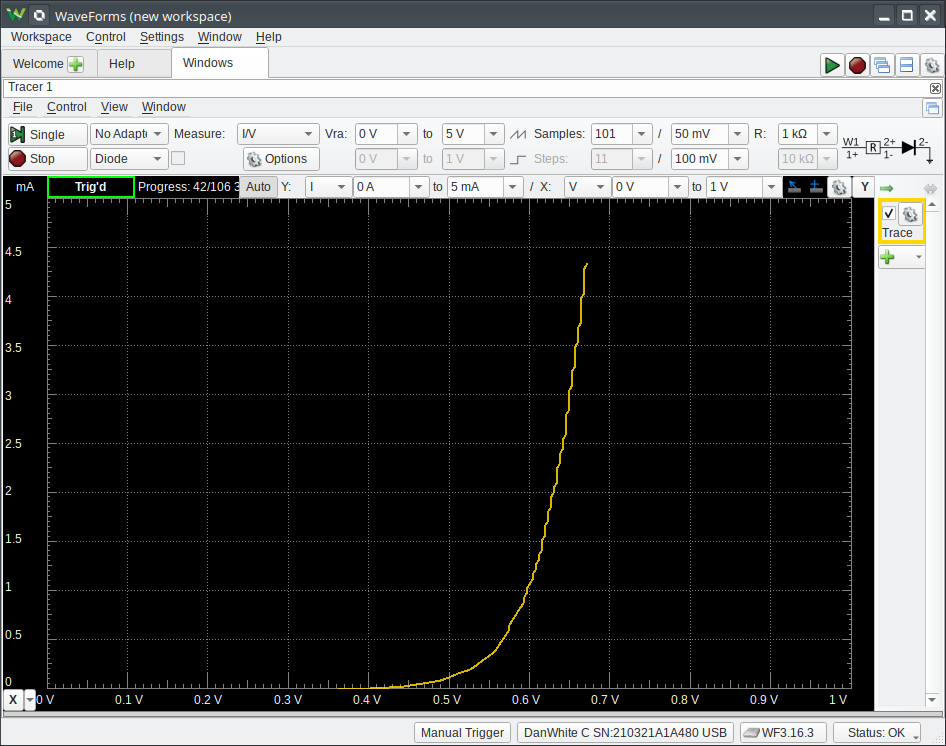
Make it easier to see relative changes and TURN OFF auto-scaling of the plot. Un-click the Auto button and set the X- and Y- scales to those shown at the top edge of the black plot display.
Click the green “+” below Trace and select Add Trace as Reference.
This will take a snapshot of your current (yellow) curve and display it as an overlay in cyan.
Change the reference’s name from Ref 1 to the name of the diode model in the circuit.
You can snapshot as many of these references as you wish. You can even export and later import the data to archive your data and compare curves from other experiments. Try this out to see how it works!
| Opening the Export window for a trace Stops the instrument. Don’t forget to Run again! |
While you are showing both the live trace and a reference trace:
-
Pinch the diode with your fingers to change its temperature (you could also carefully blow warm air across it).
-
What happens to the curve? Do this several times and formulate an opinion before continuing.
3. Background
Now that you know what real diode I/V curves should look like, we will take a side trip into a useful concept and then come back to make measurements of these diode’s I/V curves manually.
Why do this the hard way?
-
It gives us an excuse to generate log-spaced experimental data in a 1-2-5 sequence.
-
Practice using good measurement hygeine to obtain quality data (since you know what the results should be ahead of time).
-
Experience using a non-linear device in a circuit.

3.1. Log spacing

We will now take a step back from technical details to consider a concept important to Engineer-Think:
Log(arithmic) spacing
Many quantities and measurements originate from exponential or power law type functions (like \(Y = K\cdot a^x\)). It is therefore natural to plot these values using logarithmic scales (semilogy, semilogx, or loglog in Matlab-speak). The Wikipedia entry: Logarithmic scale gives examples of common log-scaled quantities.
Plots of engineering data and curves (like those in datasheets) use axes scaled using a combination of linear and log spacing for the vertical and horizontal scales so that the expected curve (ideal behavior) is a line. This allows the reader to easily see deviations from the line to better understand the non-ideal characteristics of the real device. E.g. over which range of currents the diode behaves most like the Shockley equation.
|
Do this
Open the datasheet diode_1N4004_ONsemi.pdf.
Find the ratio of figures which use at least one log-spaced axis to the total number of figures.
|
Two principles about plots and experiment design:
-
Plots of measured data (scatter plots) are generally easier to read and interpret if their points are evenly-spaced on one or both of the axes.
-
It is often up to the person doing the experiment to determine the exact points (or conditions) at which to record measurement data.
It is useful to choose measurement points at logarithmically/exponentially-spaced values if that data is expected to follow some exponential or power law (like a diode). This, combined with log-spaced plot axes, yields data points spread evenly across the abcissa[3] instead of being all bunched to one side.
Open Matlab and make this plot. Same data but different spacing.
x = [1 : 20];
figure(); plot(x, 1, '.b'); title('Even spacing')
figure(); semilogx(x, 1, '.b'); title('Bunched spacing')
3.2. The 1-2-5 sequence
The 1-2-5 sequence is a useful trick for quickly generating roughly log-spaced numbers by hand.
There are plenty of computer tools which generate log-spaced sequences of numbers, such as Matlab’s logspace() or Numpy (Python)'s numpy.logspace().
The focus today is for when the precise values are not important.
Exactly uniform log-spacing with 3 numbers per decade (factor of 10) is
Which is the sequence 1.000, 2.154, 4.652, 10.000, and so on. However, for the purpose of merely selecting points to measure, this is still more precision than needed.
→ The 1-2-5 sequence is simply these 3 log-spaced numbers per decade, rounded to integers.
An example is selecting log-spaced voltages for testing: 100 mV, 200 mV, 500 mV, 1 V, 2 V, 5 V, 10 V, etc.
| Another easily-remembered sequence that you’re likely already familiar with is the 3-4-5 right triangle. |
|
E-series for ECEs
The GEM 166 (Junior) Lab has every E12 value of resistor from 10 Ω to 10 MΩ, and either E3 or E6 spacing of capacitor and inductor stock values. Vishay’s list of standard values (PDF) lists all of the numbers in the E(3, 6, 12, 24), and E(48, 96, 192) series. Look at the document to see why they are grouped that way. Memorize the E12 series so you don’t need to walk back and forth between the supply cabinet and your desk.[4] |
3.3. 1-2-5 implementation notes
What follows are ideas and not THE STEPS YOU MUST FOLLOW EXACTLY. Pay attention to the differences between
-
selecting a target,
-
predicting a result (however imprecise), and
-
measuring a quantity in reality.
This is a good application for the 1-2-5 sequence idea!
Remember: the goal is to collect a set of (iD, vD) points that, when plotted on a semilog-y scale, will be approximately evenly spaced. Here is the Prof. White strategy:[5]
-
Select the desired starting current: 10 μA.
-
Start with the voltage source
Vsset to 1 V -
Guess a diode voltage vD of 0.4 V (you can’t calculate this voltage since you don’t know IS and η). You will get better at predicting this voltage, for now just roll with this one.[6]
-
Compute the
R1andR2resistance implied by these conditions, then select closest E12 resistor value. Measure and record the true value of these resistors.[7]
Measure the voltage source’s value and vD for each diode. Record these in your spreadsheet along with the resistor values and also create a column to compute each diode’s current from the two voltages.
-
Change the voltage source
Vsto 2 V, then 5 V, then 10 V, then 20 V, recording the resulting vD's at each step. Use this information to compute \(i_D\) (remember Ohm’s law?).
The diode voltage does not change much, since it varies with a \(\mathop{log}(I_D)\) shape, and therefore iD increases at roughly the same rate as the voltage source (which we are increasing with log-spacing). This combination gives us log-spaced current values with very little effort!
Problem: the power supply maxes out at 20 V, so you can’t continue the 1-2-5 pattern to 50 V, 100 V, etc.
-
Reset the voltage source
Vsback to 1 V and choose a diode current to target that is one more log-spaced increment larger than your last measured value.
Use the last measured value of vD (no need to guess!), and “calculate” a new resistor value that yields this current.[9]
-
Repeat the 1-2-5 sequence with the voltage source again.
(Can you intuitively explain why this second resistor value is about \(100\times\) smaller than the original value?) Choose a third resistor value if the ending current isn’t at least 20 mA.

4. Procedure
4.1. Task 1

| Est. time |
20 min |
Measure points on the \(i_D\) vs. \(v_D\) curves of the 1N4148 and 1N34A diodes for currents spanning at least 3 orders of magnitude, from around 10 μA up to around 50 mA.
Section § 3.3 covers some techniques for conveniently and rapidly obtaining these measurements that will yield good data. Go read it now.
It is wise to plot these data as you record them. Even better is to first plot the data from WaveForms as an overlay. Use Microsoft Excel, Google Sheets, a MATLAB script, or other data plotting tool of your choice.
4.2. Task 2
For the zener diode. Measure the iD vs. vD curve over a range of -10 mA to 10 mA. This is a 3.6 V zener diode so you will see the normal forward-bias diode characteristic for vD>0 and the reverse breakdown around 3.6 V.
Use the same circuit as Figure 4 but also make VS to be negative. You want enough data points so your plot traces the curve of Figure 5. Your challenge is to create measurement conditions so that your data points are equal-ish spaced along the I/V curve’s path.
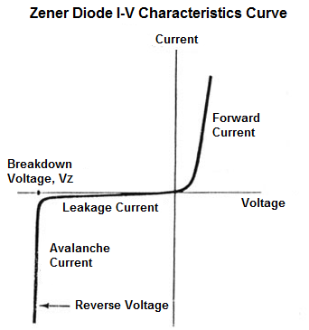
-
How many points do you need to measure so that your plotted dots trace out the important aspects of the zener diode’s characteristic curve? This decision is up to you and your partner. Choose a Goldilocks number.[10]
4.3. Analysis and visualization
4.3.1. From Task 1
-
Figure 1
Create a figure that contains all of your WaveForms' Tracer data and your manually-measured data points.
-
Use a continuous line style with no data markers for the WaveForms data
-
Use a marker-only style (no connecting line) for the 1-2-5 measured data for the same diode. Use the same color so that the curve and points visually belong to each other.
Use linear axes for both current on the vertical axis and voltage on the horizontal axis. Include a legend so the reader knows which curve/data is from which diode model.
The figure should be about as wide as your (PDF) page and have an appropriate height that makes it look good and be easy to read. (portrait height is probably way too tall)
-
Figure 2
This figure contains the same data as Figure 1, but uses a log-scale for the vertical (current) axis.
Manually-measured data points that are not close to the corresponding WaveForms Tracer data are an indication that something in your measurements and/or calculations are not correct.
Go back and re-measure if necessary.
-
Parameter estimation
For each diode with WaveForms Tracer data, find (estimate) the parameters IS and n which best fit the diode equation:
What was the temperature of the diodes during the measurements? You need that information to know VT.
The Microsoft Excel or Google Sheets trend line functionality can help with this fitting.
An alternative is to export your data columns to a .csv file and do the analysis and plotting in Matlab or other software.
Third alternative is to guess-and-check values for IS and n in a spreadsheet while plotting the equation on the same plot as your data; this is sometimes the quickest way.
| This equation is of the general form \(y = A \cdot \exp(B \cdot x)\). |
Briefly describe your procedure to get these parameter estimates, possibly with an example. Report your parameter estimates for each diode to 2 significant digits in a table.[11]
5. Report
Your report is to be a 3-page document submitted in PDF format.
These are high-value figures — make them good looking with proper labels, a title, legend, line and marker format, etc. It will take a good amount of time to do this, which is why your submission isn’t asking for other work.
You do not have a reporting responsibility for the activities in § 6. They are examples of diodes in common circuits and are included for the experience and are not circuits that you must build now. We will both build+measure and analyze these later.
6. Diode circuits
| This section is preview of work you will do in the near future. You may begin working on this now if you wish. It is NOT part of the Lab 2 reporting. |
You are encouraged to use your AD2 for this section. Collect the needed parts and do this at your own convenience.
Refer to the circuits from this handout (PDF)
Very soon, you will be asked to draw the waveforms for all of the handout’s circuits from the schematics only. Today, you are building the circuits, applying input signal waveforms, and seeing the circuits give you the solution in real-time. Your hand drawings later should match at the “critical points,” where the diodes switche modes. This is a great way to check your understanding of how diodes behave in a circuit![12]
6.1. Part 3
Construct the following circuits from the in-class handout (PDF):
-
(a) half-wave rectifier
-
(g) positive clipper
-
(h) clipper
Apply a \(4\,\mathrm{V_{p-p}}\), zero-offset triangle wave at \(1\,\mathrm{kHz}\) and use the 1n4148 diodes.
For each circuit, capture both \(v_I\) and resulting \(v_O\) at the same time with an oscilloscope.
To best see and show the diodes' effect in the circuits:
-
set each channel’s zero-reference ("ground") to the middle of the screen
-
set each channel to the same vertical scale.
| The benchtop 'scopes are USB-connected to the PCs. Use the BenchVue software to connect and capture screenshots. Waveforms, for the Analog Discovery 2 also offers a screenshot feature. |
6.2. Part 4

Construct the circuit Figure 6. Vary the signal generator’s amplitude and frequency (below 1kHz and above 10 kHz) and observe the output of the. Help the situation by ensuring the \(0\,\mathrm{V}\) level and the vertical volts-per-division is the same for both oscilloscope channels.
Recall what you know about capacitors and R-C circuits. Notice that when the diode becomes reverse-biased (i.e. turns OFF), the circuit is a parallel R-C with an initial condition. Therefore, the discharge-to-zero shape is independent of the input frequency — it only depends on the time constant. Can you predict, or explain why the output waveform has that shape?