1. Lab goals
In this lab you will construct a simple 3-stage operational amplifier from discrete components and begin measuring the DC and low-frequency performance of your unit. It will provide a real-world example for our study of the major opamp specifications which are useful in selecting an appropriate part (among the hundreds of products) during the design process.
2. Procedure
2.1. Build
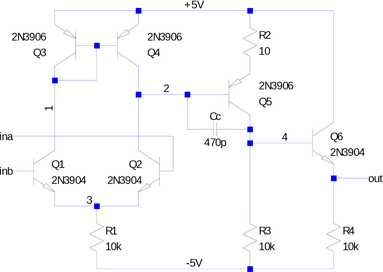
Construct the opamp of Figure 1 on a small section of breadboard.
Capacitor Cc helps to stabilize this amplifier when under feedback, but you can greatly help the situation by minimizing the length of jumper wires in your build.
-
Be sure to allow yourself easy access for replacing capacitor
Ccand for attaching probes to nodesina,inb, andout. -
Use the physically small (ceramic) capacitor type for
Cc. -
Add a power supply bypass capacitor (1 to 10 μF) between the
VccandVeenodes to help reduce the effect of the long wires connecting to the power supply. -
For each of the 3 npn transistors: use the “diode check” mode on the multimeters to measure VBE. Select the transistors with the closest values as
Q1andQ2. Since VBE is sensitive to temperature changes, it is best to minimize touching the transistors until you’ve measured them (use pliers). -
Do a similar procedure to select your
Q3andQ4pair for the current mirror.
resistor
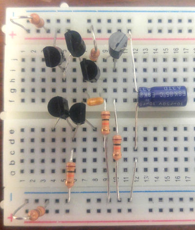
See Figure 2 for an example of pre-bending transistor leads and building the circuit in the same general arrangement as the schematic. This makes troubleshooting easier since the geometry is similar and reduces the parasitic inductances and the electric and magnetic coupling between nodes and loops.
Several of the resistors are bent to be in a vertical position. Bend and trim your resistor leads as shown in Figure 3. The right lead in the figure makes for a convenient loop for attaching probes — be strategic about which way 'round you install the resistors.
2.2. Predictions
Before applying power, it is critical that you have solid predictions of the node voltages and currents flowing in this circuit.
| Never measure a value unless and until you have an estimate of what the quantity should be. How else would you know that something is wrong?? |
-
Assume that the inputs have zero signal voltage and have a common-mode voltage of 0 V, and that the output voltage is also 0 V.
| Quantity | Predicted (V, μA) | Measured (V, μA) |
|---|---|---|
V(1) |
||
V(2) |
||
V(3) |
||
V(4) |
||
Itail, I(R1) |
||
IC(Q1) |
||
IC(Q2) |
||
IC(Q3) |
||
IC(Q4) |
||
IC(Q5) |
||
IC(Q6) |
2.3. Smoke test
The first time you apply power to a new circuit, check that the DC node voltages are “as expected”.[1]
-
Attach the +5 V and −5 V power supply connections to your amplifier.
-
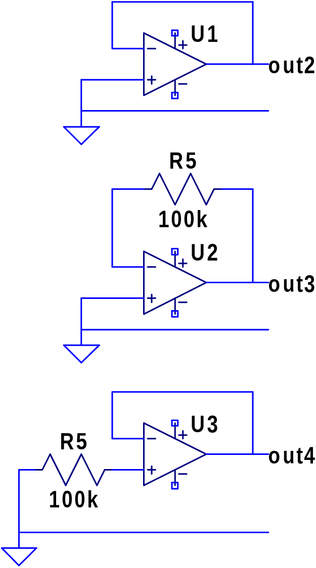
Add external wires to connect your opamp as shown in the first circuit of Figure 4 (out2) — an amplifier with voltage gain of 1 with a 0 V input. These wires are OK to be long.
Display V(out2) on an oscilloscope to verify that the amplfier is indeed quiet and not oscillating at several MHz, then use the benchtop multimeters for the DC measurements.
-
Measure the internal DC node voltages of your amplifier (nodes
1,2,3,4, and alsoout2) with respect to the 0 V node and record/compare them with your predictions.
2.4. Construct each circuit of Figure 4
Measure the value of your 100 kΩ resistor to 4 digits of precision using the benchtop multimeter.[2] Use this same physical resistor for all parts of Figure 4.
-
For each of the Figure 4 configurations, use the benchtop multimeter to measure the following DC voltages:
-
VoutN
-
Vina (+ input)
-
Vinb (- input)
-
VR, the voltage across the 100 kΩ resistor
R5. Be clear about the sign of this voltage!
-
-
You will use these numbers to help extract (compute) values for your opamp’s datasheet. You should have these numbers available to you for the next class time.
-
Current into each of the + input and − input.
-
Input offset voltage (should be zero when "amplifying" and input of 0 V — the
out2circuit).
-
|
If you are using your AD3 instead of lab equipment to make precise mV-level DC measurements
(only do this if you are unable to use the lab equipment)
|
2.5. Make an opamp-based amplifier!
Briefly review AN-7 — Typical Operational Amplifier Applications.
Can you make an amplfier with a voltage gain of +10 V/V?
Use your opamp instead of an integrated circuit opamp.
The feedback network’s equivalent resistance, as seen by the opamp’s output, should be greater than 5× 10 kΩ since the current sinking performance[3] is limited by the internal 10 kΩ R4.
| Demonstrate this by amplifying a 1 kHz input signal centered around 0 V. |