1. Supplies
-
Analog Discovery 2
-
breadboard
-
3× "jellybean" pnp transistors
-
3× "jellybean" npn transistors
-
3× 10 kΩ resistors
-
47 Ω resistor
-
10 Ω resistor
-
50 kΩ potentiometer
-
470 pF capacitor (small ceramic). (OK to be ±1 value increment)
2. Review formulas
2.1. Filters
1-pole RC high-pass filter:
1-pole RC low-pass filter:
2.2. Op-amp DC response
If you make the following assumptions:
-
The open-loop gain Av0 is large enough, which means \(\gg \left(1 + \frac{R_2}{R_1}\right)\)
-
The opamp’s open-loop output impedance Zout is low enough, or much less than the impedance seen by the output node (for this lab = 50 047 Ω). (the above equation \(\eqref{dcout}\) already sets \(Z_{out} \rightarrow 0\))
The total non-inverting opamp output from the input signal and DC errors VOS and (IB, IOS) ←→ (IB+, IB-) is:
-
\(R_{eq+}\) and \(R_{eq-}\) are the impedances seen by the + and - input terminals of the opamp.
2.3. Op-amp AC response
Most opamps have a dominant pole frequency response shape, where one pole dominates the response with the other poles and zeros near or obove than the unity-gain frequency fT.
The handout from day28 (Wednesday) discrete-opamp-ss-analysis.pdf

Use the following CircuitLab setup:
The opamp model in CircuitLab conveniently allows us to set the main datasheet parameters directly, without needing to find a device part number that mostly matches. Very handy for what if experimentation.
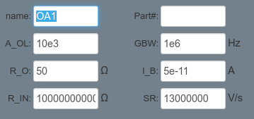
Simulate the frequency response of this circuit at various positions of the potentiometer’s wiper, parameter Rp.K (fraction of rotation 0…1).
One key result of the small-signal analysis is that the lower, dominant, pole frequency is located at
and that the Gain-Bandwidth Product (GBW) is approximately
This \(G_{m1}\) is simply the transconductance of the input differential transistor pair, which is directly proportional to bias current
Increasing GBW requires either
-
Increasing the tail current, and therefore the power supply current drawn by the opamp.
-
Decreasing Cc, which has a lower limit to maintain stability when under negative feedback.
3. Procedure
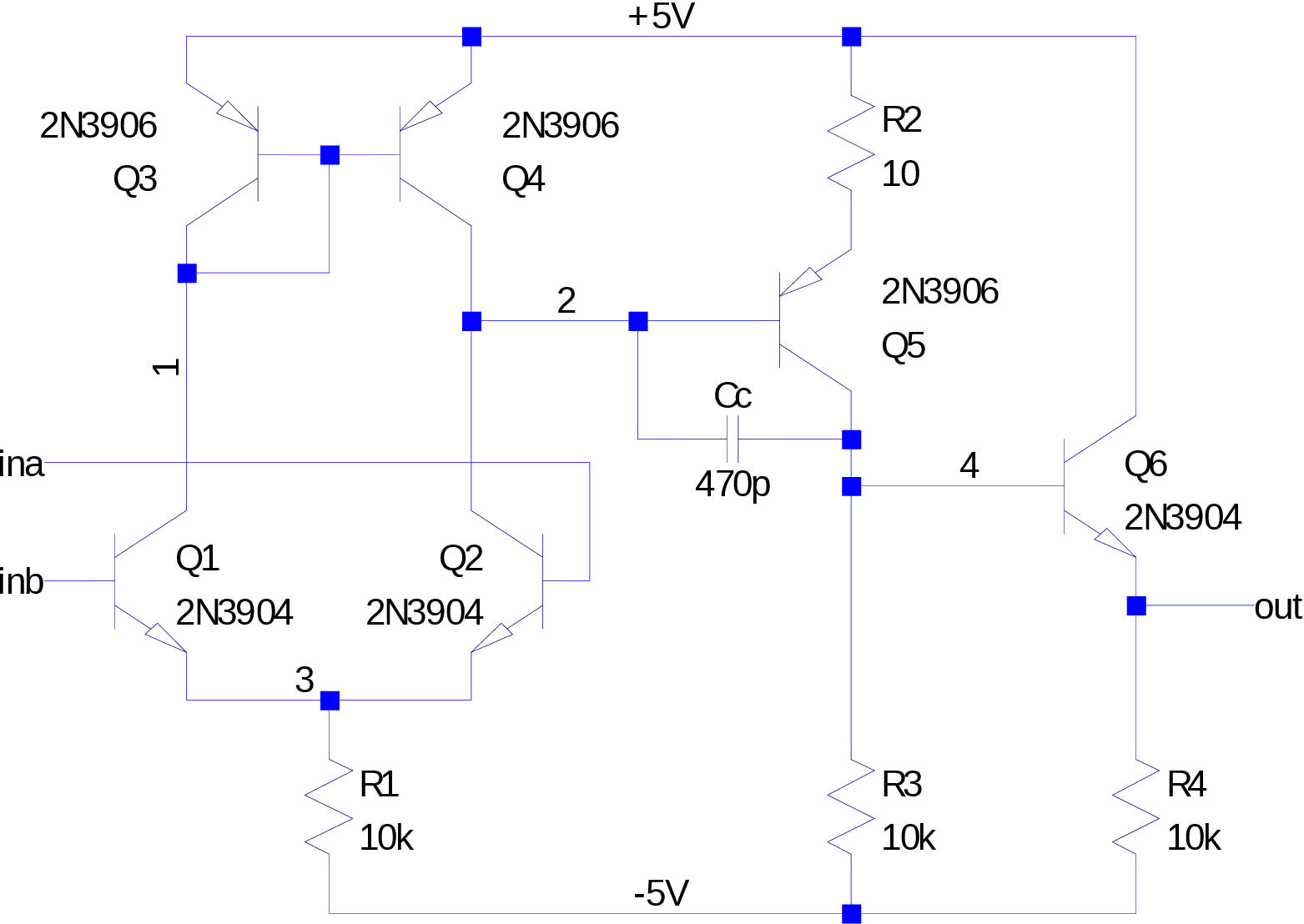

Construct your Lab 5 opamp of Figure 3. Then use this as a normal “triangle” opamp and construct the circuit of Figure 4. Instrument this circuit with your AD2 with the connections shown.
Open WaveForms and startup the Wavegen and Scope panels.
Setup the system so the amplifier output is a 1 Vp-p, 1 kHz sinusoid centered around 0 V and is operating at a gain of 100 V/V (adjust the potentiometer).
Make note of the W1 input amplitude.
Verify that the amplifier is operating correctly with a clean output waveform centered near 0 V.
Open the Network panel in WaveForms and set it up with the following parameters:
-
Upper row settings
-
Scale: Logarithmic
-
Start: 100 Hz
-
Stop: 10 MHz
-
Samples: 100
-
-
Right side settings
-
WaveGen: set to the same offset and amplitude as the current WaveGen values
-
Magnitude
-
Units: dB
-
Top: 70 dB
-
Bottom: 0 dB
-
-
Phase
-
Offset: -90°
-
Range: 180°
-
-
☆ This setup plots the magnitude and phase of your amplifier’s transfer function!
Verify that the low frequency gain is still 100 V/V, remember the conversions between dB and linear voltage units:
-
\(\text{gain (dB)} = 10 \log_{10} \Big\lbrack(\text{V/V})^2\Big\rbrack\)
-
\(\text{gain (V/V)} = \sqrt{10^{\text{(dB)}/10}}\)
or, simplified to the perhaps more familiar form:
-
\(\text{gain (dB)} = 20 \log_{10} \Big\lbrack\text{(V/V)}\Big\rbrack\)
-
\(\text{gain (V/V)} = 10^{\text{dB}/20}\)
| The frequency response plot is only valid when the system is linear, meaning the input and output signals are all within proper ranges to not clip or otherwise be distorted. One nice way to check this is to turn on the oscilloscope view at the same time. Do this by selecting menu item . |
Vary the potentiometer to set your amplifier to several low-frequency gains and measure your amplifier’s -3 dB frequency. Also compute the gain-bandwidth product at each setting (GBW is computed with gain in linear units, not dB).
| Gain (dB) | fH (-3 dB) | GBW (MHz) |
|---|---|---|
0 |
||
10 |
||
20 |
||
30 |
||
40 |
||
50 |
||
60 |
- Notice the following characteristics of these measurements
-
-
When low-frequency gain increases, the bandwidth decreases by the same proportion.
-
GBW is relatively constant.
-
GBW is nearly the same as the unity gain (1 V/V, 0 dB) frequency, fT.
-
The phase is -45° at the -3 dB frequency, exactly as predicted by the transfer function math.
-
4. Old lab notes for reference
[ the below is here simply for your edification and extra information that may be useful ]
Construct the opamp of Figure 3 on a small section of breadboard.
The capacitor Cc helps to stabilize this amplifier, but you can greatly help the situation by minimizing the length of jumper wires in the construction.
-
Be sure to allow yourself easy access for replacing capacitor
Ccand for attaching meters to nodesina,inb, andout. -
Use the physically small ceramic capacitor types for
Cc. -
Add a large capacitor (1 to 10 μF) between the
VccandVeenodes to help reduce the effect of the long wires connecting to the power supply. -
For each of the 3 npn transistors: use the “diode check” mode on the multimeters to measure VBE. Select the transistors with the closest values as
Q1andQ2. Since VBE is sensitive to temperature changes, it is best to minimize touching the transistors until you’ve measured them (use pliers). -
Do a similar procedure to select your
Q3andQ4pair.
resistor
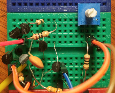
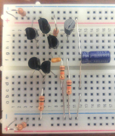
See Figure 5 for an example of pre-bending transistor leads and building the circuit in the same general arrangement as the schematic. This makes troubleshooting easier since the geometry is similar and reduces the parasitic inductances and the electric and magnetic coupling between nodes and loops.
Several of the resistors are bent to be in a vertical position. Bend and trim your resistor leads as shown in Figure 7. The right lead in the figure makes for a convenient loop for attaching probes.
References
-
[potentiometers] Bourns, The Potentiometer Handbook, https://www.bourns.com/data/global/pdfs/OnlinePotentiometerHandbook.pdf
-
[[[341-docs]]] D. White, ECE 341 reference documents folder, https://drive.google.com/folderview?id=0B5O5cSaA0tEQYVpaSnJxMGFrdHM
-
[AoE] P. Horowitz and W. Hill, The Art of Electronics, 3rd ed. Cambridge University Press, 2015. https://artofelectronics.net
-
[L-AoE] T. Hayes, Learning the Art of Electronics: A Hands-On Lab Course, Cambridge University Press, 2016. https://learningtheartofelectronics.com
-
[LEC] Tony R. Kuphaldt, Lessons in Electric Circuits, Source version: https://www.ibiblio.org/kuphaldt/electricCircuits/, All About Circuits version: https://www.allaboutcircuits.com/textbook/
-
[CL-book] Michael F. Robbins, CircuitLab, Ultimate Electronics: Practical Circuit Design and Analysis, https://www.circuitlab.com/textbook/
-
[TCA] Alfred D. Gronner, Transistor Circuit Analysis, Simon & Schuster, 1970, https://archive.org/details/TransistorCircuitAnalysis
-
[CMOS VLSI] Neil Weste and David Harris, CMOS VLSI Design - A Circuit and Systems Perspective, 4th edition. Addison-Wesley, 2011. http://pages.hmc.edu/harris/cmosvlsi/4e/index.html
-
[Tourbook] D. White, Guidebook for Electronics II. https://agnd.net/tourbook
-
[Gummel-Poon] H.K. Gummel, H.C. Poon, An Integral Charge Control Model of Bipolar Transistors. Bell System Technical Journal, 49: 5. May-June 1970 pp 827-852. https://archive.org/details/bstj49-5-827
-
[ROHM] ROHM Semiconductor, Electronics Basics, http://www.rohm.com/web/global/en_index
-
[vishay-e-series] Vishay, Standard Series Values in a Decade for Resistances and Capacitances, https://www.vishay.com/docs/28372/e-series.pdf