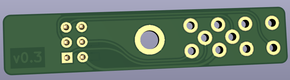
1. Programming board
PCB and soldering jig repository: https://github.com/wiredlab/xe-handheld-isp-board
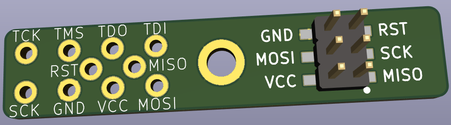
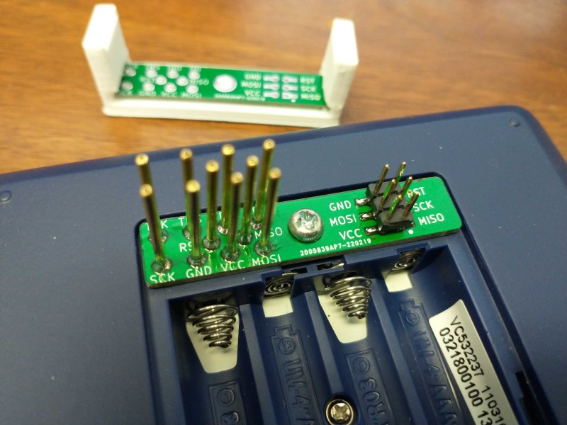
For ICP programming, only the following pins need to be soldered in, the others are for JTAG.
|
|
|
|
|
-
VCCshould be supplied via the battery. It is safer this way!
| The ICSP pins are not 5 V compatible! Ensure the signals are in the proper range before connecting your device. |
2. Explore / extract original contents
-
Following code is at https://github.com/etihwnad/srxe-notes
There are four bytes of fuses
-
lock -
efuse -
hfuse -
lfuse
Read them like:
AVRDUDE_OPTS=-p m128rfa1
AVRDUDE_OPTS+=-P usb -c usbasp-clone

.PHONY: fuses
fuses: lock.txt efuse.txt hfuse.txt lfuse.txt
	for f in $^; do echo "$$f: $$(cat $$f)"; done

lock.txt efuse.txt hfuse.txt lfuse.txt:
	avrdude $(AVRDUDE_OPTS) \
	    -U lock:r:lock.txt:b \
	    -U efuse:r:efuse.txt:b \
	    -U hfuse:r:hfuse.txt:b \
	    -U lfuse:r:lfuse.txt:b
which uses avrdude to fetch the information from an attached SRXE device and outputs:
lock.txt: 0b11001100
efuse.txt: 0b11111100
hfuse.txt: 0b10010010
lfuse.txt: 0b11101110
2.1. Lock bits
An as-received (factory) SRXE reports a lock byte with contents:
0b11001100
| bit | name | value | Description |
|---|---|---|---|
7 |
— |
1 |
— |
6 |
— |
1 |
— |
5 |
|
0 |
Boot lock |
4 |
|
0 |
Boot lock |
3 |
|
1 |
Boot lock |
2 |
|
1 |
Boot lock |
1 |
|
0 |
Lock (memory) |
0 |
|
0 |
Lock (memory) |
According to ATmega128RFA1 Datasheet, this places the device in:
{LB2, LB1} = 00→ LB Mode 3-
Further programming and verification of the Flash and EEPROM is disabled in Parallel, JTAG, and Serial Programming mode. The Boot Lock bits and Fuse bits are locked in Parallel, JTAG, and Serial Programming mode.
{BL02, BL01} = 11→ BLB0 Mode 1-
No restrictions for SPM or (E)LPM accessing the Application section.
{BL12, BL11} = 00→ BLB1 Mode 3-
SPM is not allowed to write to the Boot Loader section, and (E)LPM executing from the Application section is not allowed to read from the Boot Loader section. If Interrupt Vectors are placed in the Application section, interrupts are disabled while executing from the Boot Loader section.
2.2. Extended fuse byte
0b11111100
| bit | name | value | Description |
|---|---|---|---|
7 |
— |
1 |
— |
6 |
— |
1 |
— |
5 |
— |
1 |
— |
4 |
— |
1 |
— |
3 |
Reserved |
1 |
“Do not modify” |
2 |
|
1 |
Brown-out Detector trigger level |
1 |
|
0 |
Brown-out Detector trigger level |
0 |
|
0 |
Brown-out Detector trigger level |
BODLEVEL = 100-
Typical VBOD = 2.0 V
2.3. High fuse byte
0b10010010
| bit | name | value | Description |
|---|---|---|---|
7 |
|
1 |
Enable on-chip debugging (→ disabled) |
6 |
|
0 |
→ JTAG enabled |
5 |
|
0 |
→ SPI programming enabled |
4 |
|
1 |
Watchdog Timer always on → NOT always on |
3 |
|
0 |
EEPROM is preserved through Chip Erase → yes, preserved |
2 |
|
0 |
Select boot size |
1 |
|
1 |
Select boot size |
0 |
|
0 |
Select Reset Vector → Reset vector is Bootloader start ( |
BOOTSZ = 01-
Boot size 2048 words, 16 pages.
0x0000 - 0xF7FF - Application Flash Section
0xF800 - 0xFFFF - Boot Loader Flash Section
0xF7FF - Application End
0xF800 - Bootloader Start
2.4. Low fuse byte
0b11101110
| bit | name | value | Description |
|---|---|---|---|
7 |
|
1 |
Divide clock by 8 → disabled |
6 |
|
1 |
Clock output → disabled |
5 |
|
1 |
Select start-up time |
4 |
|
0 |
Select start-up time |
3 |
|
1 |
Select Clock source |
2 |
|
1 |
Select Clock source |
1 |
|
1 |
Select Clock source |
0 |
|
0 |
Select Clock source |
SUT[1:0] = 10-
Default start up time.
CKSEL[3:0] = 1110-
Select Transceiver clock (16 MHz).
2.5. Flash and EEPROM
We can use the following (Makefile) snippet to ask for the Flash and EEPROM contents in iHEX format:
dump: flash-dump.hex eeprom-dump.hex calibration-dump.hex

%-dump.hex:
	avrdude $(AVRDUDE_OPTS) \
-U $*:r:$@:i-
avrdudereports that the Flash is empty, leaving aflash-dump.hexthat contains zero bytes of data. -
eeprom-dump.hexcontains 4 KiB of only0xFFvalues.
These results match what might be expected from LB Mode 3*, which prohibits verification (read-back) of both Flash and EEPROM.
| The only (datasheet) way to change the Lock bits is to perform a Chip Erase. |
3. Run TinyBASIC
The original instructions are at: https://www.instructables.com/SMART-Response-XE-Tiny-Basic-Port/
As a convenience, the source code for the instructions is at: https://github.com/Subsystems-us/SMART-Response-XE-Tiny-Basic-Port