1. Setup
Section 6-3 of the Electric Manual is about the preferences in Electric. There are two sets: User and Project preferences. Read about the differences in the manual.
We will use a common set of Project preferences to ensure everyone’s work will be compatible with each other.
The following two files must be in the same folder as your .jelib library file:
There is an updated user preferences file. It changes some colors and makes the Messages window part of the editing window. Download this file also, then Import this file into your Preferences, then restart Electric.
The LTspice settings use an .ini file.
-
(new) Shortcuts reference and instructions
LTspice-hotkeys.pdf -
The settings file that replaces the default
LTspiceXVII.ini
These settings files may be found in the following locations:
-
S:\COE\ECE429\classtime— NOTE: I’ve been having trouble getting a reliable connection to the S: drive. This location may not have the latest updates.
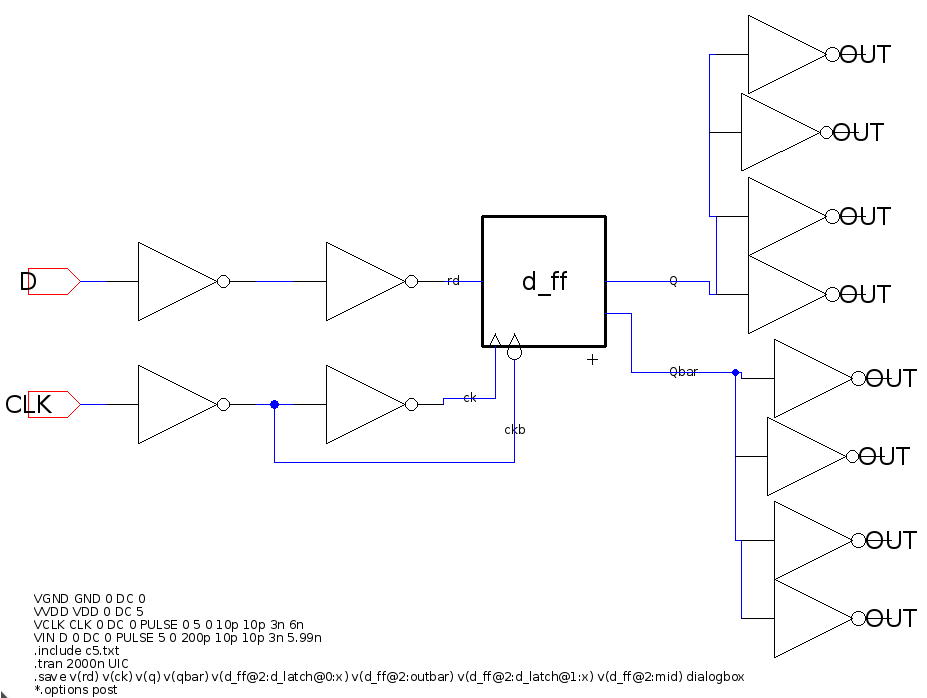
2. Master-slave DFF schematic
Construct a positive edge triggered master-slave DFF schematic in our 0.5μm technology.
Do this in a hierarchical manner, with cells of each sub-part. This means:
-
Only the inverter and transmission gate cells contain transistors! For the inverter use Wp/Wn=10/6 λ, and txgate use Wp/Wn=10/6 λ.
-
The D-latch cell contains multiple inverter cells and transmission gate cells.
-
The DFF cell contains two D-latch cell instances.
-
The test cell contains a single DFF cell and multiple inverter cells.
-
Use 2 inverters to buffer the D input pulse source to the DFF.
-
Use 2 inverters to buffer the CLK input pulse source and generate the two clock signals for the DFF.
-
Load each of the Q and Qbar DFF outputs with 4 inverters (fan out of 4) each to simulate driving realistic loads.
-
The top-level cell for simulation will look similar to the following:
-
Simulate your DFF to determine the following times:
-
Two clock-to-Q delay times (tcqr and tcqf).
-
Setup time (tsu). The minimum time between D changing and the clock edge that correctly captures the D value. (Hold time is negative for this circuit, we will simulate it later)
-
The SPICE notes page has a graphic that documents the voltage PULSE syntax.
→ Use the #chipdesign channel on Slack to help each other out. The turn-in is individual, but the figuring out how to do X or Y in Electric and LTspice can be a community effort.
3. Submission
-
Submit a single ".jelib" file that contains the following cells:
It should be possible for me to open this library from a folder that already contains the transistor models "c5.txt", find zero DRC errors, and run an LTspice simulation of your test schematic.
-
Turn in a PDF with annotated screen shots that show your measured values.
FYI, the next assignment will be to make a layout of your DFF and simulate it using the same test setup.