1. Setup
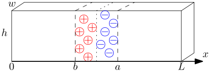
Figure 1. Imagine a bar of silicon
- Parameters[1]
-
-
w, h = 110 μm
-
L = 230 μm
-
a−b = 3.7 μm
-
ρ+ = 4.2×10¹⁵ #/cm3
-
ρ− = 1.8×10¹⁹ #/cm3
-
The region outside of [b, a] has no net charge.
-
2. Task
Plot the E-field along the x direction from 0 to L with the doping densities given.
Write a brief, self-contained, report that describes the geometry, your approach strategy to finding the E-field, the plot (completely labeled). Write a colophon section that describes the technologies and techniques you used to produce the report.
Submit a single multi-page PDF file.