Lumped element LC transmission line
1. Hardware
LC-txline.pdf - Schematic
LC-txline__Assembly.pdf - PCB layout
There are two variants available:
-
2.2 μH inductors and 47 pF capacitors.
-
10 μH inductors and 220 pF capacitors.
Drive the transmission line using the AD2’s W1 function generator using connector J1.
Leaving JP1 open, this adds a series termination resistor of 220 Ω in series with the generator output (whose output impedance is near zero.
Use the J3 to connect to scope and logic analyzer input channels.
To start:
-
Connect
C1between point [B] and GND. -
Connect
C2between point [G] and GND.
2. Analysis
-
Compute the characteristic impedance of the line Zc.
-
Compute the propagation delay in seconds per stage, and total delay from [B] to [G].
3. Measurements
3.1. DC
-
Measure the series resistance from [B] to [G] and find the average series resistance per stage, this is largely due to the inductor series resistance. Compare this to the datasheet’s claim for the two variants (2.2 μH and 10 μH).
2310271620_Sunlord-MCL1608S100MT_C51942_annotated.pdf
3.2. Pulses
Place a jumper in the Term position of J4 to add a 220 Ω resistance to terminate the line at the end (point [G]).
-
Generate a square pulse which is shorter than the total delay of the line (about 20% works well). Measure the propagation delay of the line from [B] to [G] and compare to the predicted value.
-
Keep oscilloscope input
C1at the input to the line and move inputC2to the other positions C, D, E, and F. What changes at each position?
Move the J4 jumper to the Open position.
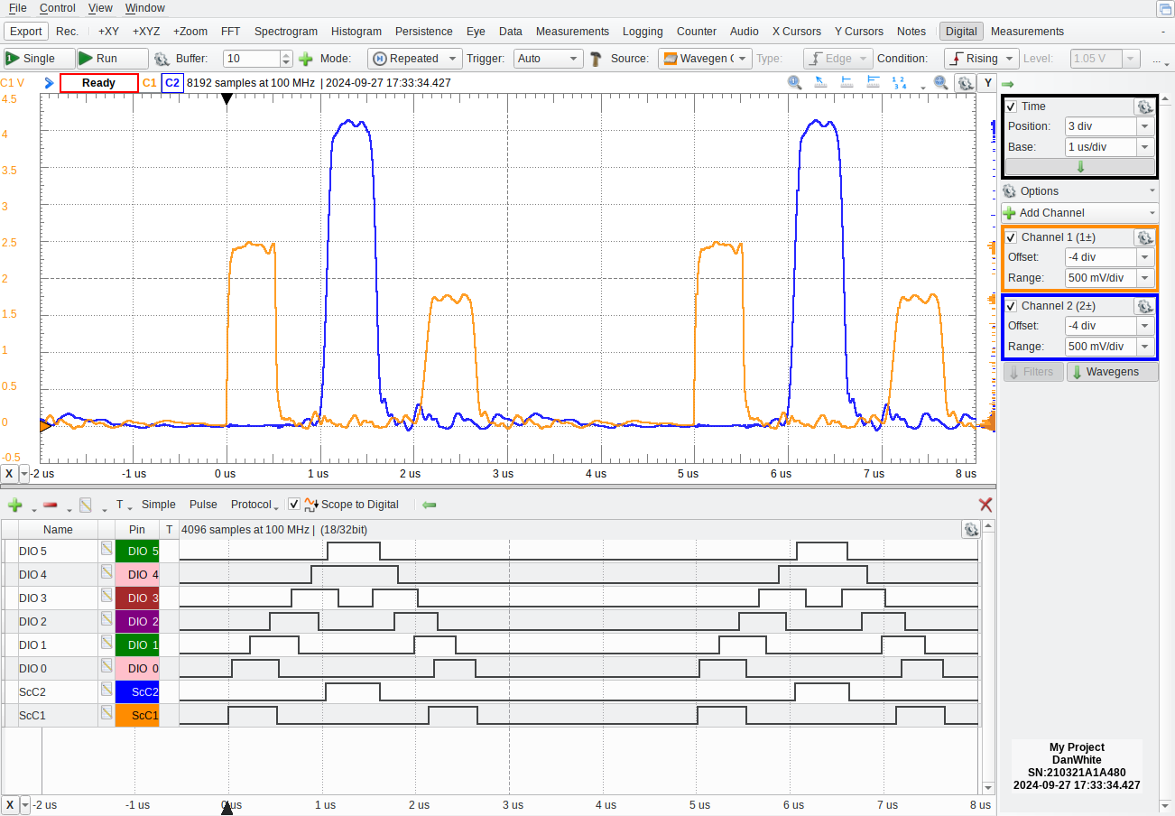
In Figure 1 the output waveform was set to be a 0-5 V pulse of 500 ns width and (repetition) frequency 200 kHz. You can display the logic analyzer on the same pane as the oscilloscope by selecting the Digital button (upper-right) and adding channels as appropriate.
-
Set up your system to show similar waveforms in real time.
-
Describe why the pulse at [B] is about 2.5 V, the peak on
C2at [G] is only about 4.1 V even though the line is open-circuited, and the reflected pulse has decreased to about 1.7 V by the left side of the transmission line. Defend your description by using circuit analysis and numbers.
Finally, move the J4 jumper to the Short position.
-
Why is point [G] always zero?
-
What does the reflected pulse look like in this situation?
Move the J4 jumper back to the Open postion.
Lengthen the function generator’s pulse so that it is at least 2× wider than the line delay.
-
Construct a bounce diagram of this line.
-
Left edge is point [B]
-
Right edge is point [G]
-
Points C, D, E, F are proportionally distributed along the length.
-
Draw a pulse that starts at B and propagates to the end of the line at G, encounters an open circuit, and reflects back towards the generator. Carefully sketch to scale what the voltage at the points along the line look like as a function of time (oscilloscope style). Use your physical line to cross-check your hand drawings of this combination of bounce diagram and time-domain plots.
3.3. Frequency response
-
Use your AD2 to plot the transfer function (the Network took in Waveforms) of the line when terminated with its characteristic impedance (Term jumper). Keep the
W1at point [A] but put input channel 1 on point [B], input channel 2 is at point [G]. -
How does the transfer function change when you don’t terminate the line (Open jumper)?