A project to create a continuity "beeper" for low resistances. Such a tool is useful for tracing circuits.
Originally an example project for ECE 322: ece322-proj-shortsquawker
Part 1
Initial features and requirements
Design requirements and features. Specifications that achieve these goals.
Features for later:
-
Battery powered. No dedicated power switch(?)
-
Turn on by shorting the probes. Pin change interrupt from deep sleep?
-
Auto turn off when idle
Minimum viable prototype
ADC value controls output square wave. This also makes an audible voltmeter. Come back to this idea later for another tool or extra operation mode.
ADC setup
timer0 setup for sample rate tick
Input circuit design
The core functionality of this device is that it takes an analog input voltage and outputs a frequency proportional to the input. This device is an ohmmeter for measuring resistance, specifically small values below X Ω or so. Eventually we’ll need to decide what this threshold X is for sounding a tone just like a continuity checker does.
To measure resistance, we will source a current, $I_{test}$ that flows through the test (small) resistance. This develops a voltage across $R_{test}$, which is then converted by the ADC into an integer.

We need to start somewhere to get a handle on what a feasible test current is and the level of resolution to expect from the system.
Here is an inventory of capabilities provided by the ATtiny85’s ADC peripheral:
-
Optional differential amplifier with ×1 and ×20 gain options.
-
10-bit converter having 1024 steps
-
Voltage reference options:
-
Internal 1.1 V
-
Internal 2.56 V
-
External pin
-
VCC, the power supply voltage
-
We don’t want the system to be dependent on the exact power supply voltage, nor do we have a particular need for the extra accuracy of an external reference, so the internal 1.1 or 2.56 V references are the remaining options.
Combined with the amplifier gains of ×1 and ×20, we get the following set of input voltage increments per least significant bit (LSb):
-
1.1 V / 1 / 1024 counts = 1.07 mV / LSb
-
1.1 / 20 / 1024 = 53.7 μV
-
2.56 / 1 / 1024 = 2.5 mV
-
2.56 / 20 / 1024 = 125 μV
If we want X mΩ / count resolution, then the test current should be:
Without other opinions, let’s target 1 mΩ per LSb, giving a maximum resistance of 1.023 Ω (first increment is 0):
-
1.1 V and 1x: 1.07 A
-
1.1 V and 20x: 53.7 mA
-
2.56 V and 1x: 2.5 A
-
2.56 V and 20x: 125 mA
If our goal is battery power and we are unwilling to make DC-DC buck converter to efficiently deliver these currents, then we should plan to always use the ×20 amplifier gain setting. One counterpoint to remember is that this current only flows when there is continuity between the probes, which is usually short for a device that makes obnoxious beeps and squawks. Since finding shorts is the entire purpose then we don’t feel quite so bad with this situation.
These currents scale inversely with the desired X mΩ / LSb specification. For example, for 10 mΩ/count, at the most sensitive setting of Vref=1.1 V and ×20 gain, the current is 5.4 mA and has a full-scale reading of 10 Ω.
Zoom back out to our intended use-case and purpose of this device for detecting relative differences in small resistances and consider a few points of reference:
-
A 6 mil trace on a PCB with copper thickness of 1 oz / sqft (a common size) has resistance of about 30 mΩ / cm.
-
The contact resistance between a (nice Molex KK 254 series) wire-to-board connector for 0.1 inch spaced headers is specified as a maximum of 10 mΩ.
-
"DuPont" jumper wires have a resistance of about 2 mΩ / cm or 20 mΩ per 10 cm piece, not including the contact resistance at each end.
Let’s split the difference and target 5 mΩ / LSb for now, therefore requiring a 10.7 mA test current. This can be supplied through a resistor of Rsource = VCC / 10.7 mA. Whoops, what is the power supply voltage VCC?
Back up to the end goal of this being powered by batteries and not via USB (5V) that will be used for development.
A fresh alkaline battery (e.g. AA or AAA) is 1.5 V and drops to about 0.9 V when considered discharged. Three of these in series yields a battery pack voltage from 4.5 down to 2.7 V.
Notice that the ATtiny85 (not the 85V) is specified for power supply voltages from 2.7 up to 5.5 V. Newer devices (including the 85V) are specified down to 1.8 V. It is no coincidence that these minimum voltages correspond to the end of life voltages of two and three-cell alkaline battery packs — it is by design.
Another consideration, while it is relevant, is Power supply current scales like
What if we use a power supply voltage held at 2.7 V independent of battery charge by using a low-dropout regulator (LDO). According to Figure 22-3, page 173, this reduces the power supply current due to the CPU from 4.5 mA down to 2.5 mA. This 44% reduction in power supply current may be a worthy effort. May, because we’ve not listed out all the ways we draw power supply current yet.
So, if the power supply voltage is fixed to 2.7 V and we want a probe test current of about 10.7 mA, then the resistance needs to be (the results are calculated using precise values, but displayed to 3 digits):
Before searching for a 251 Ω resistor, let’s go back to the datasheet and pursue an idea:
-
Using a GPIO pin to output this 2.7 V also allows us to configure that pin as an input and switch on a pull-up resistor. This pull-up resistor would then be in series with Rsource.
-
Two modes: a low precision continuity beeper mode and a high precision audible milliohm meter.
-
or for a way to inject a logic signal into a circuit as a janky square wave signal generator,
-
or other ideas …
Can this pin even output 10 mA?
Let’s check the ultimate guide: the Absolute Maximum Ratings Table 21.1, page 161, which says "DC current per I/O pin of 40 mA." So at least this won’t damage the chip.
Also remember that the output pin isn’t a perfect voltage source and therefore has non-zero output resistance. Scroll down some more in the datasheet to section §22.6 "Pin Driver Strength" and to Figure 22-21. "I/O Pin Output Voltage vs. Source Current (VCC = 3V).""
At 10 mA source current, the output voltage drops from 3.0 to about 2.6 V. This implies an effective Thevenin-equivalent output resistance of around 40 Ω, which is in series with the added Rtest resistor to achieve the 251 Ω needed to make our 5 mΩ per count resolution.
Therefore, we actually should to use a 251 - 40 = 211 Ω resistance. The closest E12 standard value is 220, so this gives Rsource = 260 Ω, a test current of 10.4 mA, and a resolution of 5.17 mΩ per LSb.
-
Do an experiment to verify this result!
The pull-up resistor has a nominal value around 40 kΩ, giving a resolution of about 0.8 Ω per LSb and a maximum value of just over 800 Ω.
Our input schematic then looks like:
 Switch
 SW1 is toggled by changing the pin to an output and setting high (Rout) or making the pin an input and enabling the pull-up resistor (Rpu).
| at this point in the design, we still haven’t assigned the pins to the MCU. We should not get too carried away since there are only 5 or 6 available on the ATtiny85. |
ADC pins
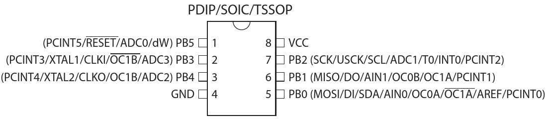
Table 10-3 Port B Pins Alternate Functions in section §10.3.1 page 60 lists the functions available at each Port B pin (the only port).
Next in our pin assignments is to see which pins are routed to the ADC peripheral.
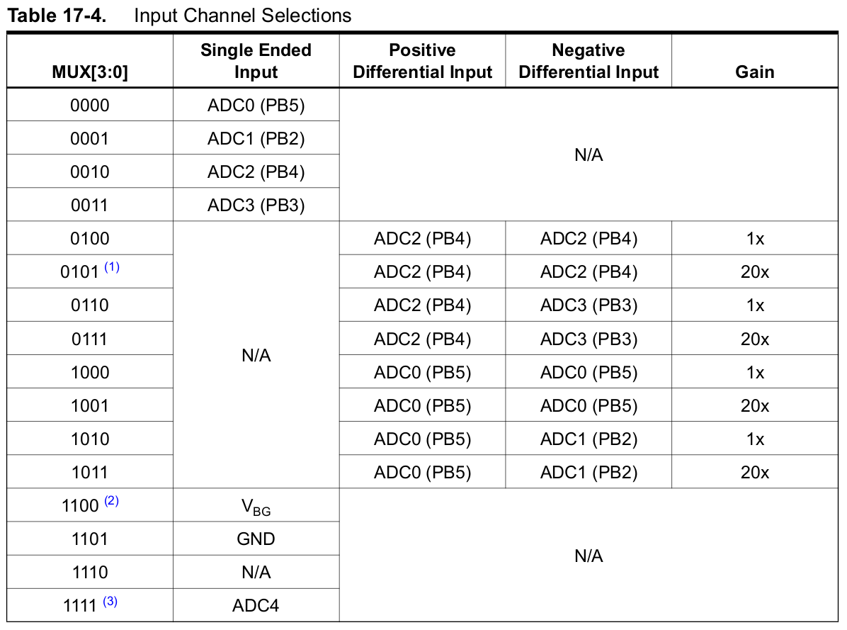
We are using the ×20 gain from the differential amplifier and so only have four lines in the input multiplexer table to consider.
Wherein we notice that half of the lines use the same pin for both + and − amplifier inputs (0101: PB4 - PB4 and 1001: PB5 - PB5).
These are useful for determining the offset in the system so it can be subtracted from real measurements.
Options for differential input pairs are then:
-
PB4 - PB3 -
PB5 - PB2
Referring to the Port B pin mapping, we see that PB5 is the RESET pin and therefore have no decision to make.
The ADC differential inputs are on pins PB4 - PB3 and are selected by MUx[3:0] = 0110 or 0111 for gains of ×1 or ×20, respectively.
Output signal generator
It is convenient to have a peripheral handle the output signal generation instead of needing to bit-bang the output pin in software. Fortunately, most timer peripherals can do this and the ATtiny85 is no exception.
There are two timers available on the MCU with slightly different features. One will be for output signals and the other will generate periodic interrupts for the input processing.
The first implementation will simply generate a 50% duty cycle square wave. However, we will later (try to) replace this signal with a PWM-based waveform generator. That needs a PWM period that is much faster than the desired output frequency.
Of the two timers available, Timer1 has an interesting capability to be clocked faster than the CPU, at up to 64 MHz. Since Timer1 uses an 8-bit counter, the maximum PWM frequency is 250 kHz, which will be plenty good for audio-frequency waveforms.
For the time being, we will only use the output compare unit(s) configured to toggle the output pin.
PLL clock
Datasheet section §6.1 Figure 6-1 on page 23 and more specifically, section §6.1.5 "Internal PLL for Fast Peripheral Clock Generation" describes the hardware.
The Timer1 documentation in section §12.2.1 simply says we need to first enable the PLL (PLLE), wait for it to start up, then select the PCK clock source for Timer1 by setting the PCKE bit in register PLLCSR.
User input
A simple button should provide enough options for a user to interact with the device. Using the internal pull-up resistor, we can simply connect a button between a pin and GND.
Additionally, remember that the two probes can also influence operational modes. For example, if the probes are open-circuit for a long time, then the system can automatically go to sleep and wake up under certain conditions such as a button press or shorting the probes (for a certain time).
We will use a state machine to manage the user interaction and actions. This is how we think about the usage, so we’ll structure the code in a similar manner.
System tick and sample rates
There are several actions that should happen regularly in our system:
-
Check and respond to user input. For human-perceived instantaneous response, we should respond to input in less than 50 ms.
-
Measure the input voltage (corresponding to a Rtest resistance) with the ADC.
-
Output a periodic signal to the speaker.
Evenly-spaced ADC samples engages discrete-time signal processing ideas — a good thing. Sampling the ADC faster allows us some overhead to filter the result (average) to avoid too much output frequency jitter due to noise.
The output signal can be handled by the timer hardware, so doesn’t really need to be handled directly. However, the updates to the timer registers should be evenly-spaced for the same ease-of-analysis reasons as the ADC rate.
Pin assignments
As is typical for a MCU, each individual physical pin has a few available functions and connects to only some subset of peripheral signals.
Inventory our needs and options:
-
-
and − ADC input
-
PB4andPB3
-
-
-
Speaker output
-
PB1orPB4
-
-
Rsource pin (output 1 or pull-up resistor)
-
PB0orPB2
-
-
User input button
-
PB0orPB2
-
… and we’re out of pins unless we disable the RESET pin and lose debugWIRE and system reset functionality.
It’s obvious is that we can’t use PB4 for the speaker output since it conflicts with the only feasible ADC pins.
The final decision is where the user input button and Rsource pins are assigned.
The test current flows through Rsource whose other end is attached to the PB4 node.
It would be convenient to use package pin 5 (PB0) for the Rsource pin so the resistor could wrap around the end of the package without crossing over the speaker output pin as it would need to do if we chose PB2.