In this lab, we will measure the current-voltage characteristics of pn junction diodes using AC signals, review preferred numbers, and send signals through several diode circuit configurations.
1. Equipment
-
Benchtop oscilloscope
-
Adjustable power supply, 0…20 V
-
1N4148silicon pn junction diode -
1N4004silicon pn junction diode -
1N4007silicon pn junction diode -
1N5817silicon Schottky diode -
2× 1 kΩ or 1.2 kΩ resistors
-
33 μF capacitor (or larger)
2. Background
2.1. Signal notation
Any signal can be decomposed into its average (DC) part and its varying (AC) part. The capitalization of both the variable and its subscript specifies which quantity the term represents.
The four possible combinations of upper and lower case have the following usual meanings, and will be consistently used in this course:
-
\(\large{\mathrm{lower}_\mathrm{UPPER}}\) - total signal (as measured by an oscilloscope with DC coupling)
-
\(\large{\mathrm{UPPER}_\mathrm{UPPER}}\) - DC or average part
-
\(\large{\mathrm{lower}_\mathrm{lower}}\) - AC or small-signal part
-
\(\large{\mathrm{UPPER}_\mathrm{lower}}\) - complex-valued phasor
2.2. Diode: a current-controlled resistance?

2.2.1. Small-signal analysis
Small-signal analysis is a technique/trick to understand how a circuit behaves for small variations around a particular fixed, or DC, operating point. This is especially useful when the circuit includes non-linear elements like diodes and transistors, where it is impossible to arrive at a closed-form (symbolic) solution to the circuit.
|
Remember linear circuits from ECE 263/264: there is no concept of “small” or “large”, since the circuit works the same at any amplitude. This is the very definition of linearity. |
The diode current is well approximated by the Shockley equation, n is called the ideality factor and is typically ≈2 at low currents for the 1N4148:
Find the slope of this function by differentiating the diode current with respect to the changes in applied voltage (vd) around the DC operating point (VD): (Pay close attention to the capitalization! Look at the connection between each step!)
This is conductance (G = A/V) with in siemens (S), sometimes called ℧ mhos. Alternatively, we may write this as a small-signal resistance (incremental slope of the \(v_D \, / \, i_D\) curve):
We will use this relationship to predict and measure this small-signal resistance when used in a current-controlled voltage divider circuit.
| Figure 1 is the graphical version of this math. |
2.2.2. Application: analog audio equipment
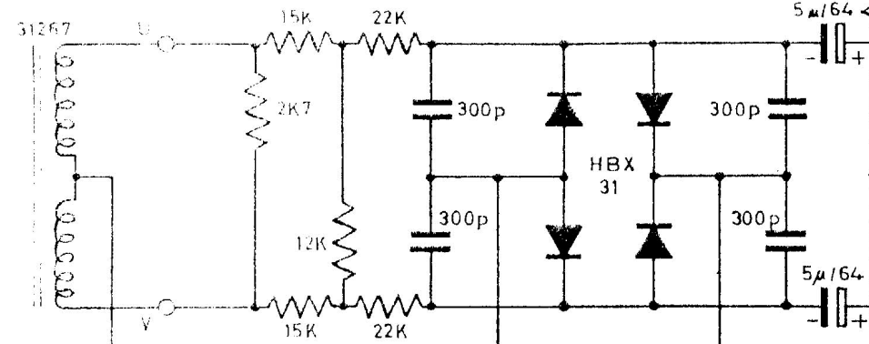
A slightly more sophisticated version of this type of circuit is used as the gain control element (volume) in several classic and modern dynamic range compressors used in audio recording and production. One still-in-production device is the Neve 2254/R (check out its current price or what the an original sells for).
Complete schematics for the Neve 2254/R are posted to the GDrive documents folder, the last page shows the portion implementing the resistor-diode voltage divider stage reproduced in Figure 3

2.2.3. Radio-frequency variable attenuator
The structure (p — intrinsic — n) type diode behaves like a normal pn junction, but stores lots of charge due to the middle layer of un-doped silicon.[1] The following documents are excelent references about the use of P-I-N diodes in radio frequency systems.
2.2.4. Radio-frequency switch
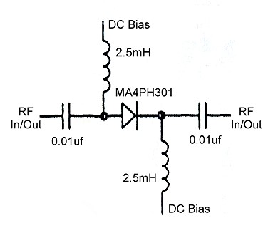
This property of controlling the incremental (or small-signal) resistance of a diode by varying the current through it allows one to only use 2 controlling currents. One state is zero current and the other is some large current value. This turns the diode into a switch whose state is controlled by the current through the diode — no current is an open circuit and large current is a small resistance.
Using a diode as a open/closed switch is quite common in radio frequency (RF) circuits as an alternative to using mechanical switches for routing signals. The figure shows a diode being used as a switch in series with the input/output. When there is no DC bias current the switch is OFF and little signal passes. When DC current is flowing, the diode is in the ON state and acts like a short-circuit letting signals pass through.
Capacitors and inductors are used to separate the AC high frequency signal path from the DC current required to turn the diode ON or OFF. The figure above came from the excellent notes of Greg Lata, amateur radio call sign AA8V:
Another reference for how PIN (p-type, intrinsic, n-type structure) diodes are used in switching radio signals is from Skyworks:
2.3. Capacitor behavior review
“Capacitor’s law” describes the relationship between current and voltage for a capacitor:
Consider what is happening with equation \(\eqref{cdvdt}\). When the voltage across a capacitor is constant, what is the current through it? (… zero) There is another circuit element that has zero current through it for any value of voltage → an open-circuit.
So, a capacitor looks like or behaves like an open-circuit at DC.
You also see this in the complex-valued impedance (Z) of a capacitor. Start by taking the laplace transform of equation \(\eqref{cdvdt}\):
What happens to ZC when the frequency goes to zero? What is the “resistance” of an open-circuit?
Now, let’s consider what happens at high frequencies.
It is easiest to see this effect in the impedance ZC. As frequency increases, the impedance drops in magnitude.
At some high enough frequency, \(\left|Z_C\right| = 500\,\mathrm{\Omega}\), which for this situation is:
Suppose that the frequency is 10× this value, about 100 Hz. The capacitor’s impedance is 10× smaller or about 50 Ω. Again, increase the frequency by 10× and the capacitor impedance is now down around 5 Ω.
Remember that this capacitor is in series with R1 from Figure 5.
You can see that adding 5 Ω to 1 kΩ still gives a series impedance of about 1 kΩ.
What other circuit element do you know where you can put it in series with something else and have no effect?
→ a short-circuit !
So, a capacitor looks like or behaves like a short-circuit at high (enough) frequencies.
These two approximations are useful in understanding what is happening in the Figure 5 circuit’s operation.
3. Procedure
3.1. Configuration

Construct the circuit shown above.
Note: the capacitor is an electrolytic type: it must be inserted with the polarity as shown so that the DC part of the voltage across it is in the normal direction. If the DC voltage is opposite, the capacitor "leaks" and allows a small current to flow (which is not ideal capacitor behavior).
Be sure to display both the zero-volt reference and each channel’s waveform on screen at the same time.
|
| The following settings are important and greatly affect the quality of your measurements. |
- Channel 1 settings
-
-
Use a normal oscilloscope probe
-
DC coupling
-
Bandwidth (BW) limit on (under the individual channel settings menu)
-
- Channel 2 settings
-
-
Use a plain BNC-to-grabber cable, not an oscilloscope probe. The probes reduce the signal by x10 before sending to the 'scope; because the signals are small to start with, this reduces our ability to see tiny amplitude signals.
-
AC coupling
-
Bandwidth (BW) limit on
-
in the channel’s "Probe" sub-menu, ensure the probe is set to \(1.00\, : \, 1\)
-
- Other settings
-
-
Touch the [Acquire] button: Mode → High Resolution
-
Signal generator settings:
-
200 mVp-p
-
zero offset sinusoid
-
1.0 kHz
-
-
Use the 0—20V DC power supply for \(V_{DC}\)
-
First connect both Channel 1 and Channel 2 to \(v_{in}\) to verify that the input signal is indeed 200 mVp-p as expected.
Then move both the Channel 1 and Channel 2 probes so that both probes are measuring the voltage across the diode \(v_D\).
With the above setup, Channel 1 is displaying the total voltage \(v_D\) and Channel 2 is displaying only the variations about the average \(v_d\). (note the captitalization, refer to § 2.1)
3.2. Task
Vary the DC power supply voltage so that the DC current through the diode varies over about 2 decades, ranging from around 0.1 mA through 10 mA.
Measure the AC amplitude of the output sine wave with the oscilloscope’s Measure functionality set on "AC RMS - N cycles" for at least 8 different currents. Use the easy 1-2-5 technique from the previous lab to yield a logarithmic spacing of 0.1, 0.2, 0.5, 1, 2, 5 mA … diode currents.
For each DC condition, record:
-
\(V_{DC}\) - DC power supply voltage
-
\(V_{D}\) - the DC part of the voltage across the diode.[2]
-
\(v_{in}\) - the signal generator amplitude in units of \(\mathrm{V_{\mathrm{RMS}}}\). This amplitude never changes, so just convert 200 mVp-p to VRMS. Read more about this “RMS” thing at Root Mean Square quantities, down to section 3.1
-
\(v_d\) - the AC part of the voltage across the diode, use "AC RMS"
Notice the fact that channel 1 and channel 2 are both measuring the voltage across the diode. Channel 2 is setup to show only the AC portion \(v_d\) while channel 1 is showing the total voltage \(v_D\).
4. Reverse-recovery time
4.1. Setup

Construct the circuit of Figure 6, first with a 1N4004 diode.
Setup the function generator to 5 Vp-p, zero offset square wave at 30 kHz.
Use normal oscilloscope probes for both channels.
|
This requires re-configuring the input channel settings since both channels are now using 10:1 probes. This is best done by clearing all of the scope’s settings back to factory default. → Select Default Setup then Factory Default. |
Your oscilloscope should look like Figure 7 with the 1N4004 diode:
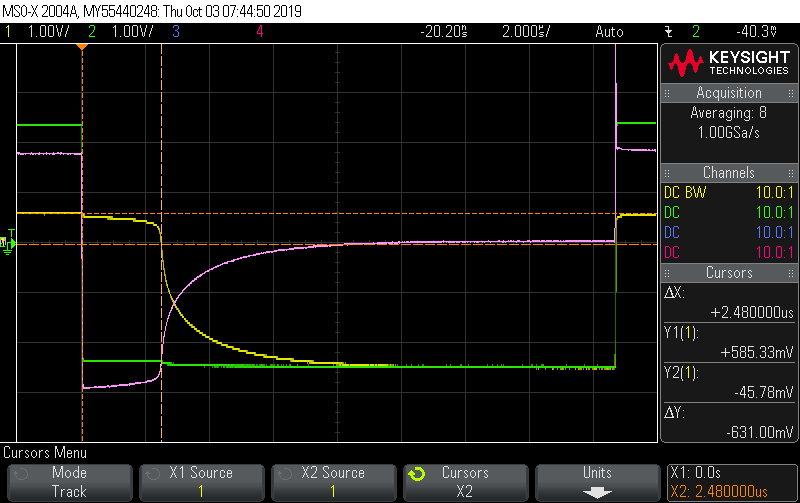
1N4004 showing 2.48 μs recovery time. (Channels 1 and 2 are swapped w.r.t the lab setup)-
Channel 1 is the input waveform.
-
Channel 2 is the diode voltage vD.
-
The magenta trace is the difference (v1 - v2). Set up this using the Math button. -→ therefore this trace is showing the diode current iD.
-
Set all scales to 1 V/div and all zero-volt levels[3] to the vertical middle of the screen.
4.2. Task
-
Measure the time it takes for a diode to become reverse-biased after carrying forward current. See Fig.5 and Fig.9 of Vishay Application Note: Rectifiers Physical Explanation for notated plots of the various reverse recovery definitions. This is not exactly the same as trr the reverse-recovery time.
| Recall that reverse-bias is when vD becomes negative. In the short transition time between forward conduction to reverse blocking mode, the diode voltage remains positive while the current is negative! This is the result of removing charge stored in the junction from diffusion currents. |
Measure this time during which the diode voltage is positive while its current is negative for the following devices:
-
1N4004silicon “standard rectifier” datasheet for1N4001through1N4007 -
1N4007 -
1N4148silicon “fast switching” datasheet -
1N5817silicon Schottky barrier diode datasheet
5. Analysis
5.1. Small-signal equivalent circuit
The concept of a “small-signal equivalent circuit” is that it’s a circuit that describes how the voltages and currents in a circuit change when the input source changes by a “small” amount.
How small is “small?”
This is a relative comparison! Generally, this means that the error between the small-signal equivalent circuit’s voltage and current values and those of the true circuit is acceptable. What is “acceptable,” then? → it depends on what you are doing or wanting from the analysis!
Obtain the small-signal equivalent circuit from the as-built Figure 5 by first considering capacitor C1.
At the input frequency of 1 kHz, the impedance of the capacitor is, if C = 220 μF:
This is much smaller in magnitude compared to R1 and R2.
It is also smaller than the small-signal resistance of the diode at the largest test current of around 10 mA:
Remember that rd is the above value or larger. So, practically, including the capacitor’s impedance in the circuit analysis has little numerical effect on the result. Therefore, round the capacitor’s impedance to zero (a.k.a. a short-cirucit).
The power supply voltage source is set to a constant (DC) value and never changes. For the small-signal equivalent circuit we are only interested in how quantities do change. → Replace the voltage source’s value with its AC value only (which is zero).
The capacitor and V-source substitutions yield Figure 8.

Next up, replace the 0 V source with a short-circuit and label the two terminals of R2 so we can keep track of what happens with it, giving Figure 9.

Replace diode D1 with its small-signal equivalent circuit.
See [_current_controlled_resistance] and equation (6) for its derivation.
Resistor R2 in the circuit can be rotated in the circuit without changing how it is connected.
Notice between Figure 9 and Figure 10 that it is still connected between node vd and the reference node.

The final small-signal equivalent circuit in Figure 10 is used to estimate the gain of the circuit for small-amplitude input signals. This circuit describes how the circuit in Figure 5 behaves for the AC portion of the voltages and currents. Every device in the full original circuit must be accounted for in the small-signal equivalent circuit!
as a function of the circuit elements and the DC current through the diode.
Remember:
-
R1andR2stayed the same and are connected to the same places. -
VDCwas pure-DC and so it’s AC model is a short-circuit. -
C1was short-circuited because, in this particular situation, it series impedance was negligible in context. -
D1, a non-linear device, was replaced by its small-signal equivalent circuit model.
Notice that rd, the diode’s small-signal equivalent resistance, is a function of the DC (average) current through the diode. This means that changing this diode DC current will change the numbers in Figure 10.
5.2. Task
Analyze the circuit of Figure 10 to find the gain of the circuit from the input vin to the output taken as vd. This will be a funciton of the DC current through the diode, ID. Assume room temperature with \(V_T = 26\,\mathrm{mV}\) and an ideality factor of n=2.
-
Plot this predicted (ideal) small-signal transfer function with log-log scaling.
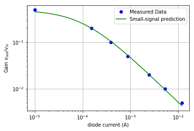
On the same plot as this predicted curve, plot your measured \(v_{d} / v_{in}\) at each measured diode DC current. Figure 11 demonstrates how this plot should look. Your measurements should be very close to the theoretical curve if you used good measurement hygiene. See Figure 11 for a representative example
Discuss your observations about the output waveform shape as the bias current varied and ranges where your measurements matched the predicted values. Given your observations with the DC-coupled Channel 3, discuss the problems this circuit injects onto the output signal if the diode current is varied rapidly to dynamically change the attenuation ratio.
6. Report
Turn in your figure showing the circuit analysis prediction of the small-signal gain calculated from figure [ss-circuit] along with your measured data as points. Use Figure 11 as a guide for this figure.
Write a few paragraphs of observations about your reverse-recovery time measurements:
-
Why are the
1N4004and1N4007values similar but the1N4007larger value? -
What does the datasheet for the
1N4148claim as the maximum reverse-recovery time? Make some engineering guesses of why your measurement was nowhere near this value. -
What about the
1N5817was/is different and why?