A project to create a continuity “beeper” for low resistances. Such a tool is useful for tracing circuits.
Originally an example project for ECE 322: ece322-proj-shortsquawker
1. Initial features and requirements
-
Two multimeter-like probes for measuring between two points on a circuit.
-
Momentary switch
-
Hold — set reference to current value.
-
Short Press — activate / deactivate alternating reference tone.
-
Tone alternates between live and reference.
-
-
-
Speaker
-
Output frequency is proportional to resistance or input voltage.
-
1.1. Minimum viable prototype
ADC value controls output square wave frequency.
Timer to control sample rate.
State machine to handle button press/hold.
1.2. Potential future features
Low power operation.
-
Battery powered. No extra power switch.
-
Turn on by shorting the probes or a button press.
-
Auto turn off when idle.
Output sounds.
-
Play reference and current tones at the same time.
-
Morse code to indicate operating mode / numerical value / ???.
-
Adjustable output volume.
2. Input circuit design
This device is an ohmmeter for measuring resistance, specifically small values below X Ω or so. The core functionality of this device is that it takes an analog input voltage and outputs a frequency proportional to the input. Eventually we’ll need to decide what this threshold X is for sounding a tone just like a continuity checker does.
- TODO
-
There is no protection thus far for situations where the two user probes are connected to weird locations.
Voltages at the input probes must be in the range [0 — VCC] V, with VCC < Vbattery.
2.1. Selecting Rsource
To measure resistance, we will source a current \(I_{test}\) that flows through the test (small) resistance. This develops a voltage across \(R_{test}\), which is then converted by the ADC into an integer.

We need to start somewhere to get a handle on what a feasible test current is and the level of resolution to expect from the system.
Here is an inventory of capabilities provided by the ATtiny85’s ADC peripheral:
-
Optional differential amplifier with ×1 and ×20 gain options.
-
10-bit converter (1024)
-
Voltage reference options:
-
Internal 1.1 V
-
Internal 2.56 V
-
External pin
-
Vcc, the power supply voltage
-
We don’t want the system to be dependent on the exact power supply voltage, nor do we have a particular need for the extra accuracy of an external reference, so the internal 1.1 or 2.56 V references are the remaining options.
Combined with the amplifier gains of ×1 and ×20, we get the following set of input voltage increments per least significant bit (LSb), ordered by size:
Vref / gain / counts = V / LSb
-
2.56 / 1 / 1024 = 2.5 mV / LSb
-
1.1 V / 1 / 1024 counts = 1.07 mV
-
2.56 / 20 / 1024 = 125 μV
-
1.1 / 20 / 1024 = 53.7 μV
If we want X mΩ / count resolution, then the test current should be:
Without other opinions, let’s target 1 mΩ per LSb, giving a maximum resistance of 1.023 Ω (first increment is 0):
-
2.56 V and 1x: 2.5 A
-
1.1 V and 1x: 1.07 A
-
2.56 V and 20x: 125 mA
-
1.1 V and 20x: 53.7 mA
If our goal is battery power and we are unwilling to use/make a DC-DC buck converter to efficiently deliver these currents, then we should plan to always use the ×20 amplifier gain setting. One counterpoint to remember is that this current only flows when there is continuity between the probes, which is usually only for a short time since the device makes obnoxious beeps and squawks. Since finding shorts is the entire purpose then we don’t feel quite so bad with this situation — battery energy is only consumed when things are active.
These currents scale inversely with the desired X mΩ / LSb specification. For example, for 10 mΩ/count, at the most sensitive setting of Vref=1.1 V and ×20 gain, the test current is 5.4 mA and has a full-scale reading of 10 Ω.
Zoom back out to collect some more information relevant for our intended use-case of detecting relative differences between small resistances and consider a few points of reference:
-
A 6 mil trace on a PCB having a copper thickness of 1 oz / sqft (a common value) has resistance of about 30 mΩ / cm.
-
The contact resistance between a (nice Molex KK 254 series) wire-to-board connector for 0.1 inch spaced headers is specified as a maximum of 10 mΩ.
-
"DuPont" jumper wires (for a breadboard) have a resistance of about 2 mΩ / cm or 20 mΩ per 10 cm piece, not including the contact resistance at each end.
Let’s split the difference and target 5 mΩ / LSb for now, therefore requiring a 10.7 mA test current. This can be supplied through a resistor of Rsource = VCC / 10.7 mA.
Whoops, what is the power supply voltage VCC?
Recall the end goal of this being powered by batteries and not via USB (5 V).
-
A fresh alkaline battery (e.g. AA or AAA) measures 1.5 V and drops to about 0.9 V when considered discharged. Three in series yields a battery pack voltage from 4.5 down to 2.7 V.
-
Notice that the ATtiny85 (not the 85V) is specified for power supply voltages from 2.7 up to 5.5 V.
-
Newer devices (including the ATtiny85V) are specified down to 1.8 V.
It is no coincidence that these minimum voltages correspond to the end of life voltages of two and three-cell alkaline battery packs — it is by design.
Another consideration, while we are considering power usage, is that power supply current scales like the following in most digital systems (C is the capacitance that is switched at a typical edge):
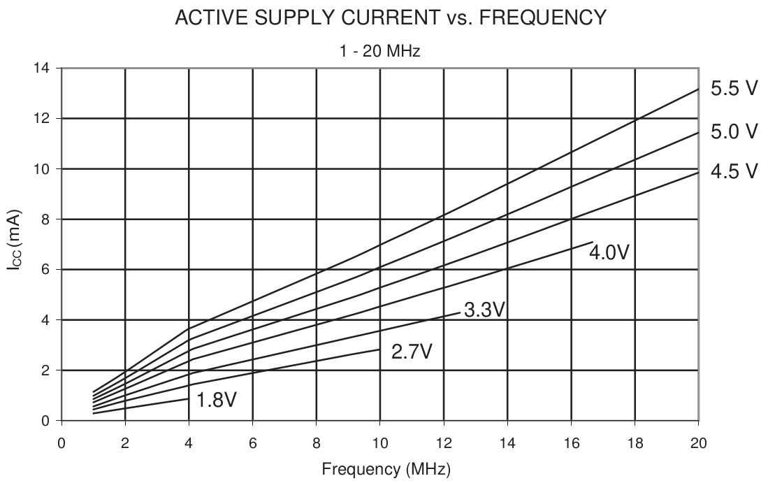
This behavior is confirmed in the ATtiny85’s datasheet, §21.1 Active Supply Current. A representative plot is Figure 22-2 on page 173 which shows that reducing the supply voltage and reducing the clock frequency both reduce the supply current when active.
What if we use a power supply voltage regulated to 2.7 V, independent of battery state of charge, by using a low-dropout regulator (LDO)? According to Figure 22-3, page 173, this reduces the power supply current due to the CPU from 4.5 mA down to 2.5 mA. This 44% reduction in power supply current may be a worthy effort.
So, if the power supply voltage is fixed to 2.7 V and we want a probe test current of about 10.7 mA (which flows only when actively probing a ≈short-circuit), then the resistance needs to be:
Before searching for a 251 Ω resistor, let’s go back to the datasheet and pursue an idea:
Using a GPIO pin to output this 2.7 V instead of connecting directly to the power supply allows us three options:
-
Drive the pin with a
1output for normal use. -
Drive the pin with a
0to zero the test current. -
Set the pin as an input with the pull-up resistor enabled, which is in series with Rsource.
This would allow two levels of precision:
-
Low precision continuity beeper mode for lower power usage.
-
High precision audible milliohm meter.
Plus provide the hardware for a feature such as using the probe to inject logic signals into a circuit.
Can this pin even output 10 mA?
Probably a wise idea to verify this before proceeding much farther.
Let’s check the ultimate guide: the datasheet’s Absolute Maximum Ratings Table 21.1, page 161, which says "DC current per I/O pin of 40 mA." So at least this won’t damage the chip.
Also remember that the output pin isn’t a perfect voltage source and therefore has some output resistance. Scroll down some more in the datasheet to section §22.6 Pin Driver Strength and to Figure 22-21. I/O Pin Output Voltage vs. Source Current (VCC = 3V).
At 10 mA source current, the output voltage drops from 3.0 to about 2.6 V. This implies an effective Thevenin-equivalent output resistance of around 40 Ω, which is in series with the added Rsource resistor to yield the 251 Ω needed to make our 5 mΩ per count resolution.
Therefore, we actually should to use a 251 - 40 = 211 Ω resistance. The closest E12 standard value is 220, so this gives:
-
Rsource = 260 Ω,
-
a test current of 10.4 mA,
-
and a resolution of 5.17 mΩ per LSb.
-
Do an experiment to verify this result!
The pull-up resistor has a nominal value around 40 kΩ, giving a resolution of about 0.8 Ω per LSb and a full-scale value of just over 800 Ω.
Our input schematic so far looks like:

Switch SW1 is toggled by changing the pin to an output and setting high (Rout) or making the pin an input and enabling the pull-up resistor (Rpu).
| At this point in the design, we still haven’t assigned the pins to the MCU. |
2.2. ADC input pins
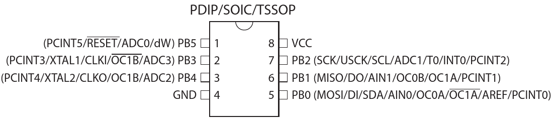
Table 10-3 Port B Pins Alternate Functions in section §10.3.1 page 60 lists the functions available at each Port B pin (the only port).
Next in our pin assignments is to see which pins are routed to the ADC peripheral.
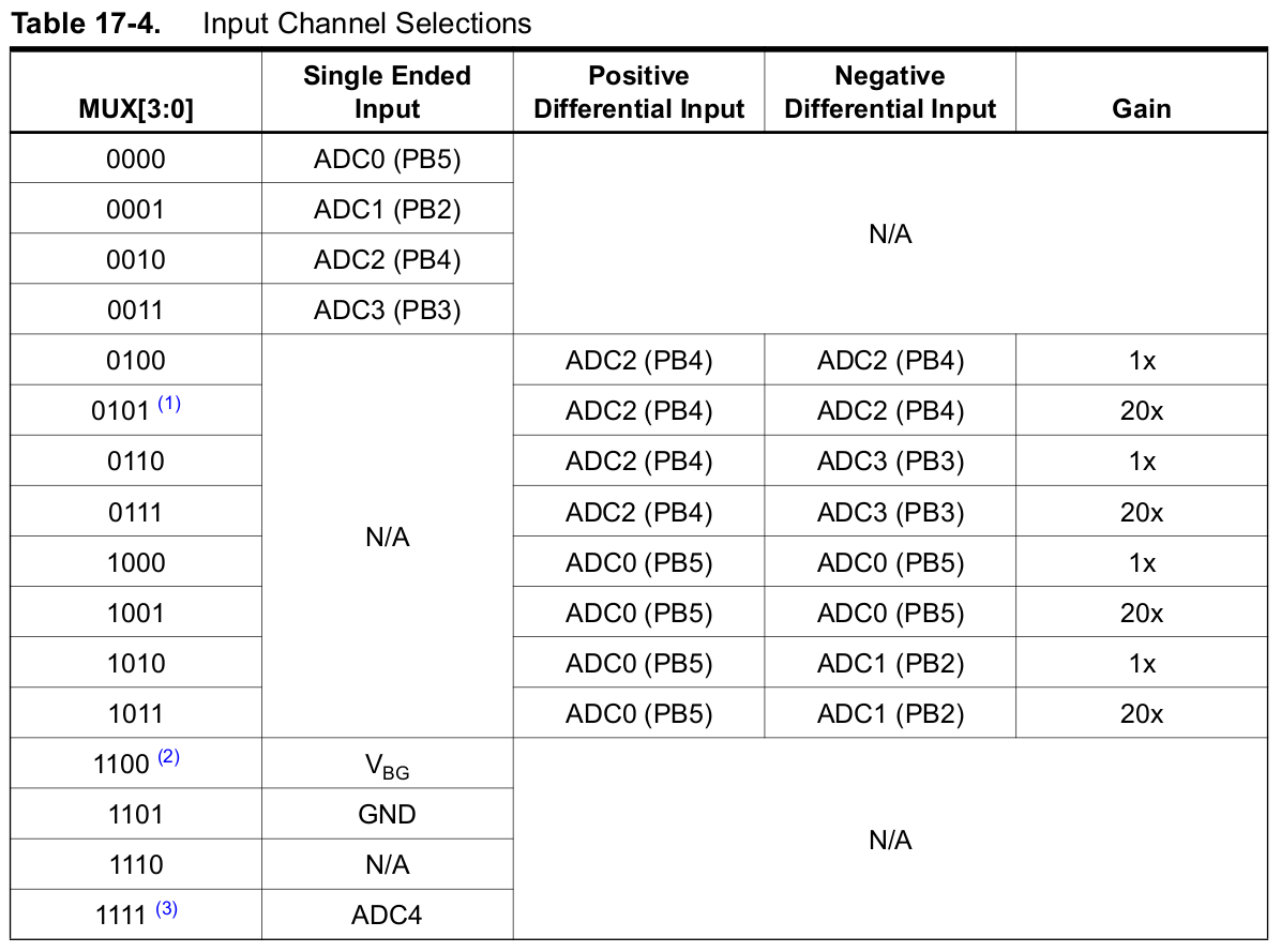
We are using the ×20 gain provided by the internal differential amplifier and so only have four lines in the input multiplexer table to consider.
Wherein we notice that half of the lines use the same pin for both + and − amplifier inputs (0101: PB4 - PB4 and 1001: PB5 - PB5).
These are useful for determining the offset in the system so it can be subtracted from real measurements.
Options for differential input pin pairs are then:
-
PB4 - PB3 -
PB5 - PB2
We recall that PB5 is the RESET pin and therefore have no decision to make if we don’t want to sacrifice RESET.
-
The ADC differential inputs are on pins
PB4 - PB3and are selected byMUx[3:0] = 0110 or 0111for gains of ×1 or ×20, respectively.
2.3. User input
We will use a state machine to manage the user interaction and actions. This is how we think about the input button’s behavior, so we’ll structure the code in the same way.
A simple button provides several options for a user to interact with the device to change its behavior. By enabling the internal pull-up resistor, we can simply connect a button between a pin and GND.
| Remember to debounce the switch before taking action or risk the firmware accepting multiple presses when the user only intended one. |
Remember that the two probes are also inputs controlled by the user. For example, if the probes are open-circuit for a long time, then the system can automatically go to sleep and wake up under certain conditions such as a button press or shorting the probes (for a certain time).
Two pins are connected to the ADC peripheral and are used in differential mode for normal operation.
Remember that you can re-configure the ADC input to measure the voltage at just one of the pins. This gives three possible measurements:
-
VPB4 − VPB3
-
VPB4 − GND
-
VPB3 − GND. Figure 7 includes resistor R3 in series with the test current so that the voltage at
PB3can be different from GND.
3. Output circuit
Unless we decide to use an LED or something else, then the only output is to drive a loudspeaker.
It is convenient (and usually best) to have a peripheral handle the output signal generation instead of needing to “bit bang” the output pin in software. Fortunately, most timer peripherals can do this and the ATtiny85 is no exception.
There are two timers available on the 'tiny85 with slightly different features. One will be for generating the speaker output signal and the other will generate periodic interrupts for the input and output sample rates.
The minimum viable implementation simply generates a 50% duty cycle square wave. However, we will later replace this signal with a PWM-based waveform generator which needs a PWM frequency much faster than the output audio frequency.
Of the two timers available, Timer1 has the interesting capability to be clocked faster than the CPU, up to 64 MHz.
Since Timer1 uses an 8-bit counter, the maximum PWM frequency is 250 kHz, which will be plenty good for audio-frequency waveforms.
Rspk: Most moving-coil loudspeakers have nominal impedances in the 4—16 Ω range. This is much too low for directly driving from an MCU pin.
For an output current of 10 mA with a supply voltage of 5 V, then the load impedance should be at least 500 Ω. Including the internal 40 Ω output impedance from § 2.1 and a speaker load of 4 Ω, then Rspk should be ≥(500 - 40 - 8) = 452 Ω.
Round to the next E12 value and set Rspk = 470 Ω. Larger values will simply make the sound output quieter.
3.1. Timer1 clock, pins, and modes
3.1.1. PLL clock
Datasheet section §6.1 Figure 6-1 on page 23 and more specifically, section §6.1.5 Internal PLL for Fast Peripheral Clock Generation describes the hardware that generates this faster clock.
The Timer1 documentation in section §12.2.1 says we need to
-
First enable the PLL (
PLLE), -
wait for it to start up,
-
then select the
PCKclock source for Timer1 by setting thePCKEbit in registerPLLCSR.
3.1.2. PWM output mode
Datasheet §12.2.2 Timer/Counter1 in PWM Mode reveals that we can do fast PWM with either or both of OCR1A and OCR1B.
Searching the Figure 5 pinout diagram shows that using OCR1B isn’t possible since it conflicts with our usage of the ADC pins.
OCR1A output via PB1 it is, then.
Select PWM mode by setting PWM1A in register TCCR1.
From the datasheet:
When set (one) this bit enables PWM mode based on comparator OCR1A in Timer/Counter1 and the counter value is reset to $00 in the CPU clock cycle after a compare match with OCR1C register value.
We will keep the value of OCR1C at its maximum of $FF so we can get a full 8-bits of duty cycle resolution.
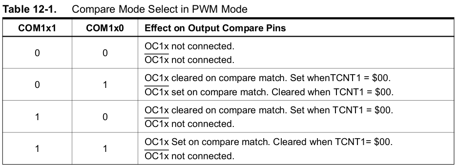
Figure 6 describes the meaning of the COM1A[1:0] bits in TCCR1 when in PWM mode.
The middle 01 and 10 lines are the most relevant to us.
-
Output pin (
PB1) is set (high) at the start of the interval, -
then cleared (low) when the timer reaches the
OCR1Avalue.
→ Then the output duty cycle is simply OCR1A / (OCR1C + 1). The +1 is from a careful reading of the datasheet :)
The distinction between COM1A[1:0] modes 01 and 10 is whether or not the \(\overline{\mathtt{OC1A}}\) signal, which is the inverse of OC1A is routed to a physical pin (PB0).
For this application, you would attach the loudspeaker between these two pins instead of wiring the speaker − to GND.
The result is doubling the voltage across the speaker and a +6 dB increase in volume.
Unfortunately, this forces us to give up either the user input button or the Rsource switching.
File the potential volume enhancement away for a rainy day and only route output signal OC1A to PB1.
4. Schematic
4.1. Pin assignments
As is typical with an MCU, each physical pin has several possible functions and connects to some subset of internal peripheral signals.
Inventory our needs and options:
-
(+ and −) ADC input
-
PB4andPB3
-
-
Speaker output
-
PB1(maybe +PB0)
-
-
Rsource pin (output 1 or pull-up resistor)
-
PB0orPB2
-
-
User input button
-
PB0orPB2
-
… and we’re out of pins unless we disable the RESET pin and lose debugWIRE or system reset functionality.
-
It’s obvious is that we can’t use
PB4for the speaker output since it conflicts with the only feasible ADC pins. -
The remaining decision is where the user input button and Rsource pins are assigned.
The test current flows through Rsource whose other end is attached to the PB4 node.
It would be convenient to use package pin 5 (PB0) for the Rsource pin so the resistor could wrap around the end of the physical package without crossing over the speaker output pin as it would need to do if we chose PB2.
Decisions:
-
→ Select
PB2for the user input pin. -
→ Select
PB0to drive the top side of Rsource.
4.2. Summary

| Function | Pin |
|---|---|
± ADC input |
|
User input button |
|
Speaker output |
|
Rsource top |
|
no-connect |
|
This pinout is for the complete device in its final form factor.
There are some changes that make developing the firmware more convenient:
The (PB4 − PB3) ADC differential input can be set to a gain of ×1 instead of ×20, then attach PB3 to GND.
Doing this makes for an input range of 0—1.1 V at PB4, therefore allowing us to attach one Wavegen channel from an AD2 to drive the input easily.
Waveforms has a “Basic” mode that uses a slider input to control the DC output voltage; set the range of the slider to be a safe 0 V to 1.2 V.
Resistor Rsource interacts with the unknown resistance Rtest being probed and is solely for sourcing a known current.
But for interacting with the firmware, only the voltage between PB4 and PB3 matters.
Therefore, Rsource may be omitted, leaving the pin PB0 uncommitted.
→ Use PB0 for a 1-pin “printf” by attaching it to an oscilloscope or logic analyzer for measuring firmware timing and getting internal state information out of the system without needing to use the debugWIRE debugging features present on the polymorphic RESET pin 1 / PB5.
5. Timer0 system tick and sample rates
There are several actions that should happen regularly in our system:
-
Check and respond to user input.
-
For human-perceived instantaneous response, we should respond to input in less than 50 ms.
-
-
Measure the input voltage (corresponding to a Rtest resistance) with the ADC.
-
This should also be human-scale instantaneous and faster than button response → around 10 ms.
-
Sampling the ADC faster allows us some overhead to low-pass filter the result (average it) to avoid too much output frequency jitter due to noise.
-
-
Output a periodic signal to the speaker. The output PWM signal can be handled by the timer hardware.
-
However, the updates to the timer registers should be evenly-spaced for the same ease-of-analysis reasons as the ADC rate.
-
The output sample rate fs (rate updating the PWM duty cycle) should be as fast as possble. This increases the frequency separation between the desired fundamental frequency f0 and its alias at fs - f0.
6. Waveform generation
Instead of outputting a square wave directly from a timer, the ShortSquawker generates sinusoids using direct digital synthesis.
Ask The Application Engineer—33: All About Direct Digital Synthesis from Analog Devices' publication Analog Dialogue.
The digtal-to-analog converter used in our case is a PWM signal whose duty cycle is proportional to the desired output voltage. Low-pass filtering this signal recovers the “analog” portion of the waveform and suppresses the many higher-frequency alias products.
6.2. Phase-Amplitude Conversion
The phase signal gets converted to a waveshape with a PAC.
On the AVR, it is convenient to have nco_phase be an 8-bit value.
The sin() then can be computed with a 256-entry look-up table instead of using a math library function call (which is very expensive).
// Returns an 8-bit resolution sinusoid.
int8_t next_output(uint16_t phase_increment) {
    static uint16_t dco_phase = 0;
    uint8_t out_phase;

    // NCO phase wraps around
    dco_phase += (phase_increment & 0xFFFF);

    // extract the fixed-point 8.8-bits integer part
    out_phase = (dco_phase >> 8) & 0xFF;

    // Could interpolate with the fractional part, but not now.
    return sine_table[out_phase];
}
Niels Mosely has a nice writeup about generating and using a table lookup: Sin/cos generation using table lookup and interpolation
That version uses a float table, but similar things can be done with a table of int8_t integers.
7. Similar projects
Both of these use the (analog) comparator on a 'Tiny for a binary beeper use. They also feature an auto-sleep function, where wakeup uses a pin-change interrupt.
-
wagimator: Continuity Tester based on ATtiny13A
I like the use of a pogo pin for the probe.