Structure and strategy are of utmost importance in a chip layout.
Purposes for this assignment:
-
Gain experience creating layouts of logic circuits.
-
layout geometry
1. Setup
By now you should have custom settings for both Electric and LTspice and know how they are changed and updated. See hw07 - Setup for reference.
2. Master-slave DFF layout
First: Ensure your hw07 DFF works properly as a D flip-flop.
The schematic version must be functional as a positive edge triggered DFF.
-
Create the layout of your DFF by creating layout views of the constituent cells, beginning from the lowest level of the inverter and transmission gate. Do this in a hierarchical manner, with cells of each sub-part.
-
Run DRC (shortcut F5) early and often to catch mistakes. It is pointless to have DRC errors and attempt to run a simulation.
Electric VLSI, along with every other legitimate EDA (Electronic Design Automation) tool, has a function to check that the schematic view matches the layout view. This is usually called Layout versus Schematic (LVS), but is called Network Consistency Checking (NCC) in Electric.
-
Run NCC from the Tools menu (shortcut F3) after completing the layout for each cell. Fix the issues it finds!
-
Before asking questions about NCC results, you must somehow demonstrate that you have carefully read the manual.
-
| NCC (and DRC) must pass with "exports match, topologies match, sizes match" before you move to the next higher hierarchy level. |
You will also need to draw the layout view of your testing cell with the input buffers and 4x inverters loading the Q and Qbar outputs. The top-level cell for post-layout simulation will look similar to the following:
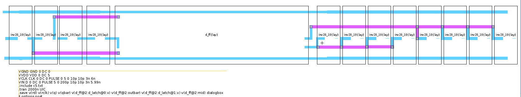
Connect the LTspice voltage sources defined in the Spice Code block to the nodes in the layout by attaching a name to the relevant arcs.[1]
3. Timing measurement simulations
Now that Electric knows the physical geometry of your circuit, it has enough information to automatically compute the parasitic resistance and capacitance in the layout. Recall that every conductor has a capacitance to other conductors, and these capacitances are not trivial at the tiny distances between devices on a chip.
The electricPrefs-ECE429-v3.xml settings you (should) have loaded, configures the Spice netlist writer in Electric to only consider transistor geometry.
Every source and drain of every transistor is a pn junction that is (should be) reverse-biased.
This reverse-bias junction capacitance is the origin of the C's at the drain/source nodes you drew in hw06.
Having accurate values for these capacitances is critical for getting realistic waveforms and delays from the simulator.
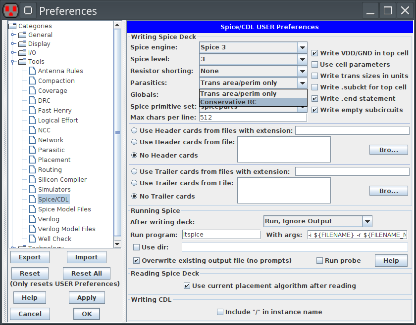
Change the parasitic extraction settings in Electric’s Tools→Spice/CDL preferences to include the resistance and capacitance of the polysilicon and metal layers. Select the "Conservative RC" option.
-
Simulate your DFF to determine the following times:
-
Two clock-to-Q delay times (tcqr and tcqf).
-
Setup time (tsu). The minimum time between D changing and the clock edge that correctly captures the D value.
-
-
Compare your post-layout times to your schematic-only times.
-
It is illegitimate to compare times that were simulated under differing conditions.[2]
-
4. Resources
4.1. Textbook
The Weste and Harris book is good to read!
-
§1.5.3 introduces layout design rules. The values are the same as our 0.5μm process.
-
§1.5.4 has good advice and strategites for gate layout.
-
§3.3 is all about design rules
4.2. agnd.net
The SPICE notes page has a graphic that documents the voltage PULSE syntax.
4.3. Other books
The website for the book CMOS Circuit Design, Layout, and Simulation at http://cmosedu.com has a collection of videos about Electric, among other things.
-
Electric_video_6demonstrates some useful layout techniques and live troubleshooting of problems you are likely to have.
4.4. Slack
→ Use the #chipdesign channel on Slack to help each other out. The turn-in is individual, but the figuring out how to do X or Y in Electric and LTspice can be a community effort.
5. Submission
Submit exactly 2 files.
-
A single PDF with a brief report of your results. Describe how you measured the requested values, e.g. text and annotated screen shots.
-
Add some discussion about the differences between the
.spinetlist file generated by Electric for the schematic design and the netlist that includes the transistor drain and source perimeters and areas, and wiring capacitances and resistances. -
This document should be complete in the sense that it is not strictly necessary to open any other files to understand what you did, how you did it, your measurement results, and discussion.
-
-
A single ".jelib" file that contains the following cells and cell views:
It should be possible for me to open this library from a folder that already contains the transistor models c5.txt and projsettings.xml, find zero DRC errors, zero NCC errors, and run an LTspice simulation of both your test cell’s schematic and layout views.