Spring 2022
1. Information
| Credits |
3 Credits |
| Prerequisites |
ECE 221, ECE 340, and instructor permission. |
| Instructor |
Dr. Dan White |
It is helpful to also be familiar with the topics of ECE 222 and ECE 424.
Lower-credit versions of this independent study are a subset of the Goals and Objectives with proportionally fewer deliverables.
2. Goals
The following are the high-level Goals, the complete Goals and Objectives are found at Goals.
2.1. G-FAB: Fabrication
Learn the fundamentals of the fabrication and physical design of integrated circuits.
2.2. G-LOGIC: Digital logic design
Design combinational and sequential digital logic (integrated) circuits.
2.3. G-SIM: Simulation
Simulate and characterize combinational and sequential circuits at the transistor and structural levels.
2.4. G-FLOW: Design flow
Use hierarchical tools and techniques to manage design complexity.
- Bottom-up
-
Transistors to macro cell libraries and process design kit (PDK)
- Top-town
-
RTL-to-GDSII using OpenLane.
3. Topics
-
Review of MOSFET physics
-
CMOS fabrication processes
Combinational logic design styles
-
Static CMOS
-
Ratioed
-
CVSL
-
Dynamic
-
Pass transistor
Sequential circuits
-
Timing
-
Latches
-
Flip-Flops
-
DFF in detail
-
setup and hold constraints
-
internal delays
-
Topics
-
Clock domains and synchronization
-
Metastability
-
-
Delay
-
RC model
-
Elmore
-
Logical effort
-
-
Power
-
Dynamic
-
Static
-
Energy-delay optimization
-
Low power techniques
-
-
Interconnect
-
Layout parasitics
-
Delay
-
-
Simulation using *SPICE (LTspice and Ngspice)
-
Transistor models
-
Parametric variation
-
Scripted measurements
-
Synthesis
-
Static timing analysis
-
Floorplanning
-
Placement
-
I/O
-
Power distribution network
-
Clock tree distribution
-
-
Routing
-
Parasitic extraction
-
Post-layout simulation
-
DRC
-
LVS
-
GDSII tapeout
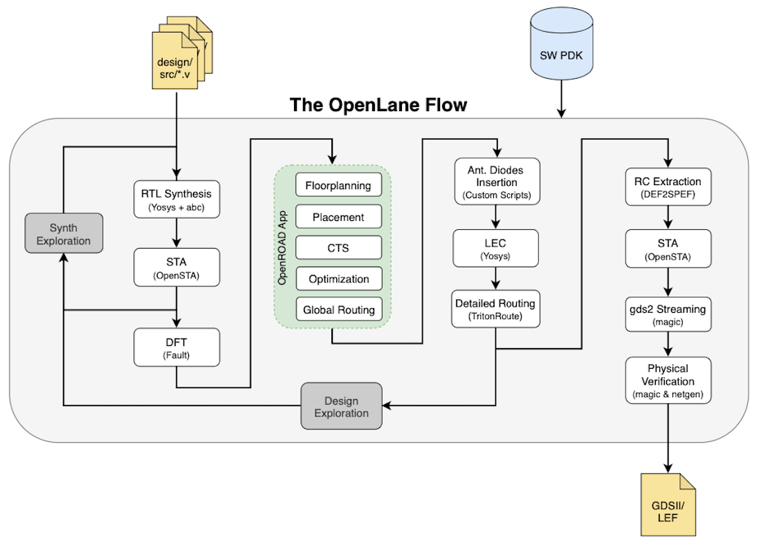
See also OpenLane Design Stages
4. Assessment
As the semester progresses, the student will assemble a portfolio of work. That work provides tangible evidence of reaching objectives that support the course’s goals found in § 2. Defined objectives are listed in this document with "OBJ-name" tags.
An Objective includes one or more Tasks
Each Objective is met by documenting the following
-
Objective name and description.
-
Link to associated Goal(s).
-
Link to associated Topic(s).
-
Report logging the Tasks completed
-
Summary notes, simulation inputs and results, analyses, graphics, code, etc.
-
Date stamps (YYYY-MM-DD format)
-
|
The Tasks in an Objective do not necessarily need to be done sequentially as a group. They may be interleaved in time with tasks from other objectives as part of the learning process. A rule-of-thumb: The tasks of an objective are equivalent to moderate-sized traditional homework problems. In fact, some objectives are appropriately set in the form of end-of-chapter exercises. TODO Example: A set of 3-4 end-of-chapter exercises |
| Specific |
simple, sensible, significant |
| Measurable |
meaningful, motivating |
| Achievable |
agreed, attainable |
| Relevant |
reasonable, realistic and resourced, results-based |
| Time-bound |
time-based, time limited, time/cost limited, timely, time-sensitive |
The course letter grade is proportional to the number of objectives met.
5. Resources
- Textbook
-
Neil Weste and David Harris, CMOS VLSI Design: A Circuits and Systems Perspective, 4th Edition. 2011 Pearson
- Slack
-
#chipdesignchannel at (valpo-engr.slack.com). Valpo Engr Slack Invite link, then join the#chipdesignchannel.