1. Learning objectives
A student who has successfully completed this course will have
-
Designed 2 PCBAs from through the: schematic - layout - ordering and fabrication - assembly - testing phases.
-
Created new schematic symbols from component datasheets.
-
Created new PCB footprints from component datasheets.
-
Evaluated component selections for ease of assembly and availablity of alternate sources.
-
Soldered through-hole and surface mount parts.
2. Syllabus
4. How to register
First, go to the following link, which lives on the Registrar’s Forms page:
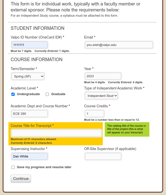
4.1. First page
Remember to use the correct semester and year!
- Course Title for Transcript
-
“PCB Design”
4.2. Second page
- Substance of Project
-
Students will learn the fundamentals of electronic circuit physical design through the schematic, printed circuit board, and assembly phases. Each will complete two projects of increasing complexity.
- Method of Evaluation
-
Student work is evaluated on acceptable completion and documentation of each phase for each of the two projects on a four-level EMRN rubric.
4.3. Third page
Upload the following PDF of the syllabus:
Attach the PDF version of the syllabus ( web syllabus )
5. Tools
-
KiCad for schematic and PCB layout.
6. Schematic basics
symbols light vs heavy symbols pins metadata multiple-part packages
pages inter-page connections
good style conventions idea: side-by-side good and bad examples good vs better
design rules ERC DRC other checks or policies use, setup why have enforced design rules?? "sign off" issues
netlists for simulation for pcb data
7. Printed Circuit Boards
7.1. Printed circuit structure
laminates
fabrication layers for photoresits
solder mask
silkscreen printing
surface finish ENIG HASL SMOBC plating
ROHS issues lead-free
7.2. Other
footprints create from scratch with datasheet from a quality library from vendor libraries built-in libraries ALWAYS cross check your libraries for accuracy, it will bite you eventually
design rules net classes current handling width spacing isolation creepage
physical clearance around hardware
package naming conventions and standards
??? IPC trainings to complete ???
through-hole typical package types DIP SIP TO-220 TO-92
surface mount package types SOIC SOT QFN BGA
floor planning strategies placement physical connectors working with an enclosure constraint mounting holes keep outs height of parts
violating design rules sign-off
8. Assembly
8.1. Soldering
-
find good tutorials for references
melting metal heat transfer is key clean tips flux
soldering iron hot air hot plate reflow oven